Spot Check pt. V
firmware repo
node.js api repo
iOS app repo
hardware repo - new hardware repo for open source Eagle schematic and layout files, schematic PDFs, BOMs, datasheets, and other notes
Previous project updates:
Overview
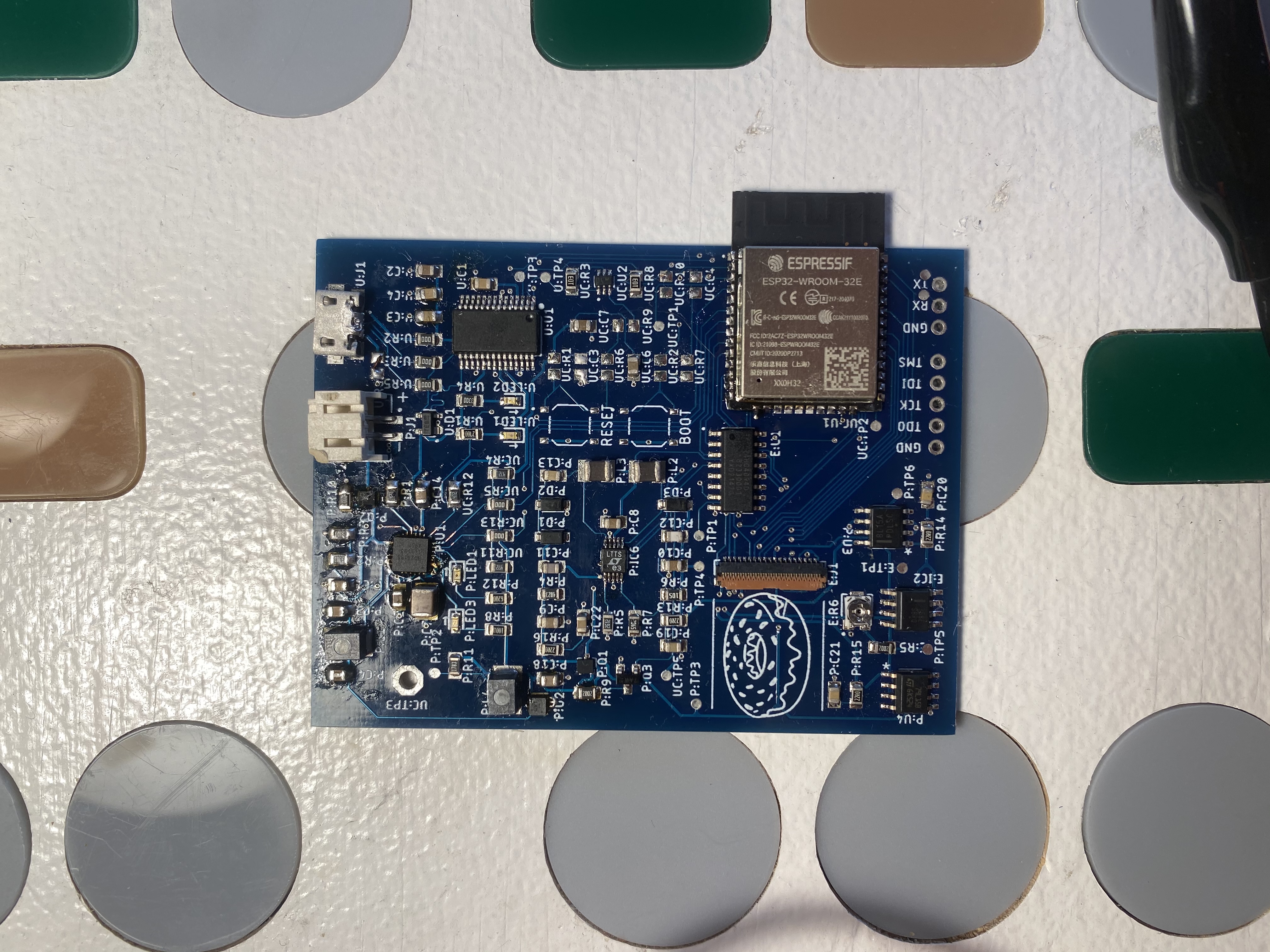
Rev. 3 packed a whole lot of changes in. Not only did I switch from scrolling LED strips to an e-ink screen as the display, but I also added battery power, charging over USB, and USB programming and communication instead of a UART header.
Was it dumb to make this many changes at once to the board? Yes.
Did I pay for it deeply at bring-up? Also yes.
Am I happy I did it? …….I think?
The main driver behind the switch from LED strips to e-ink was the awkward UX of interacting with the device within arm’s reach while still being able to read the LED strips. Since they’re best viewed from a distance, but the user needed to be close to press a button to trigger the scrolling forecast, there was a weird ‘button press then step back three steps and wait’ mechanic. I also like e-ink much more as a medium, and while it has its own assembly drawbacks, I found it much easier to deal with than bodging connections from strip to strip.
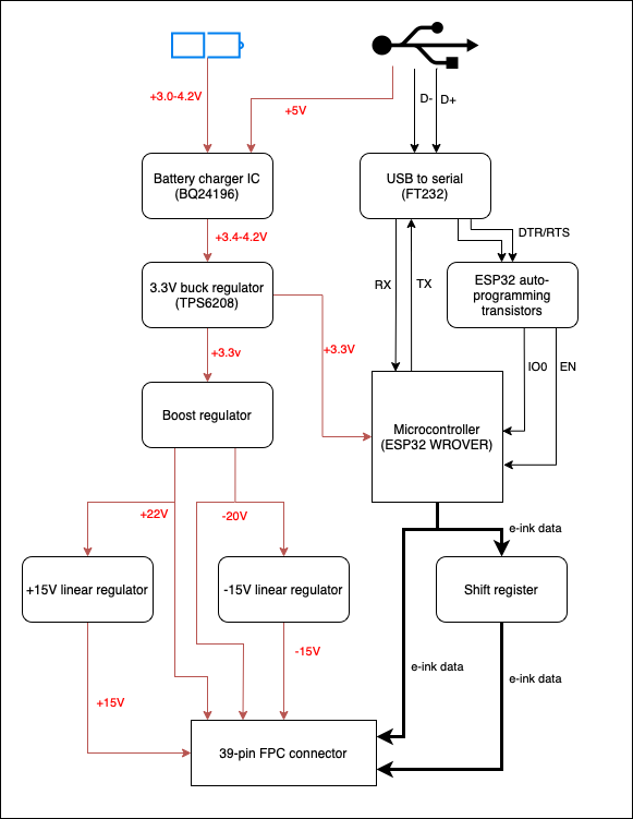
A block diagram of the hardware and subsystem connections
Along with switching to e-ink, I also wanted to make several other hardware improvements, like the USB programming and power, for a better development experience and to work on design and layout for newer areas that I hadn’t built before.
Design

The overall schematic page with each section separated into its own module
USB

There are many options for simple USB to serial converter ICs and I wasn’t picky, but the ongoing chip shortage made it very difficult to find any. I ended up going with the option from FTDI, the FT232, because I could find some on eBay for relatively inexpensive. When I say relative, I mean it was still $6 for a single 14-pin SSOP. I also knew I was taking a big risk with counterfeit parts, but it was the best option I had.
Basic USB to serial communication needs very little of the chip’s functionality: just power, ground, USB D+ and D- in, and serial TX and RX out. There are 5 configurable function pins, two of which operate as open-drain TX and RX signals by default. I connected two LED cathodes to each of these to see the transfer of data for debugging.
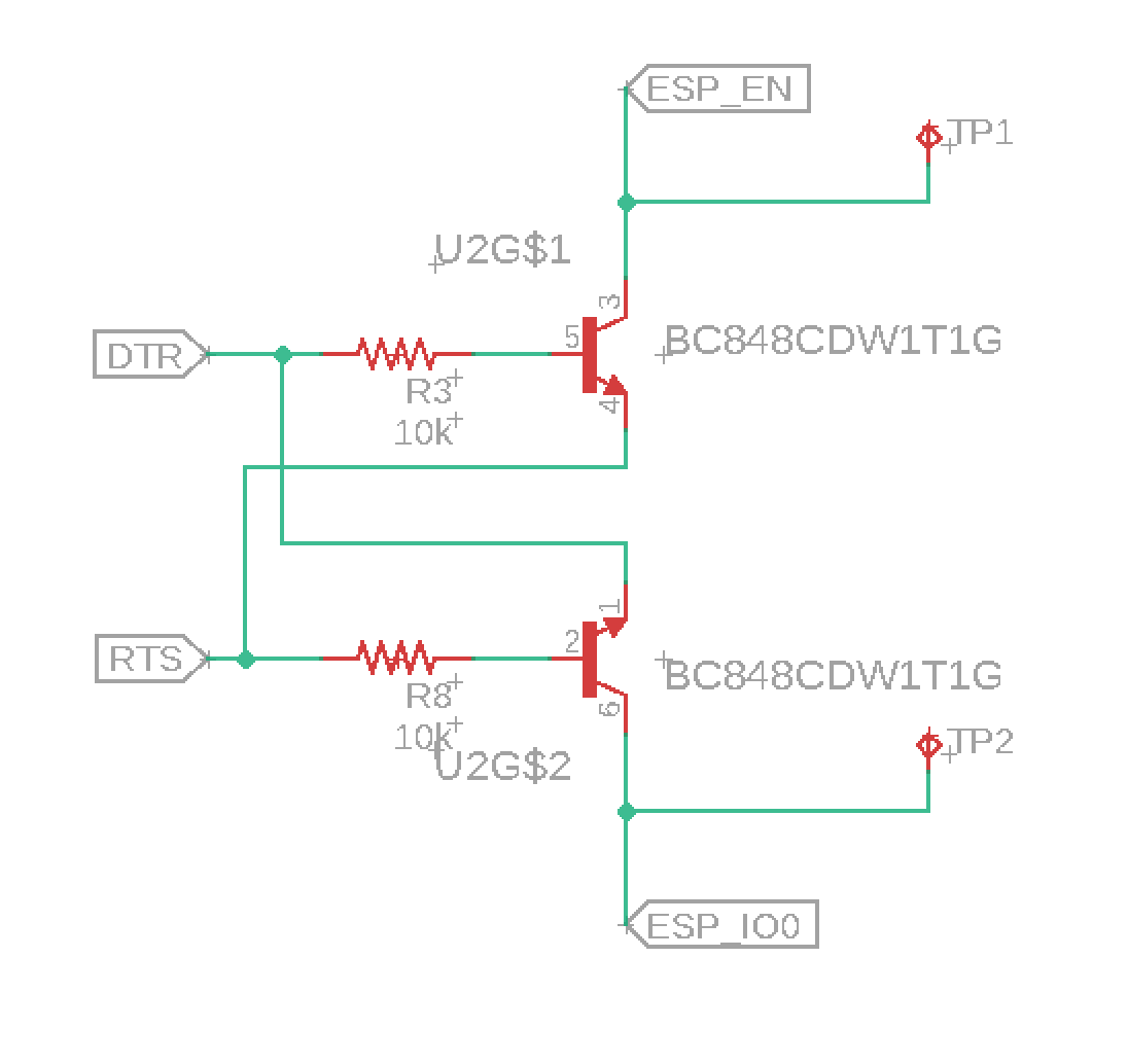
The simple auto-programming circuit for ESP32 MCUs
One bonus feature of using a USB to serial converter is that its standard RS232 logic for toggling RTS and DTR can be abused to kick the ESP32 into programming mode automatically. By wiring the DTR/RTS outputs to the IO0 and EN pins of the ESP32 in the BJT configuration seen above, the ESP32 is automatically booted into programming mode during the initial handshake process that the FT232 performs.
This means the developer doesn’t have to do the classic ‘hold BOOT0 button and press the RESET button to program the ESP32’ every single code flash or serial monitor connection. Note: this only works If there’s a large enough capacitor on the EN pin of the ESP32 since the alignment of DTR and RTS pulses is super close together.
I also added a small TVS IC on the 5V, D+, and D- from USB. I did not use the ID pin of the micro USB standard.
Power

Complete power schematic. Broken into subsections below
This was by far the most complicated part of the redesign so it makes sense that it’s the part that gave me the most headaches during bringup.
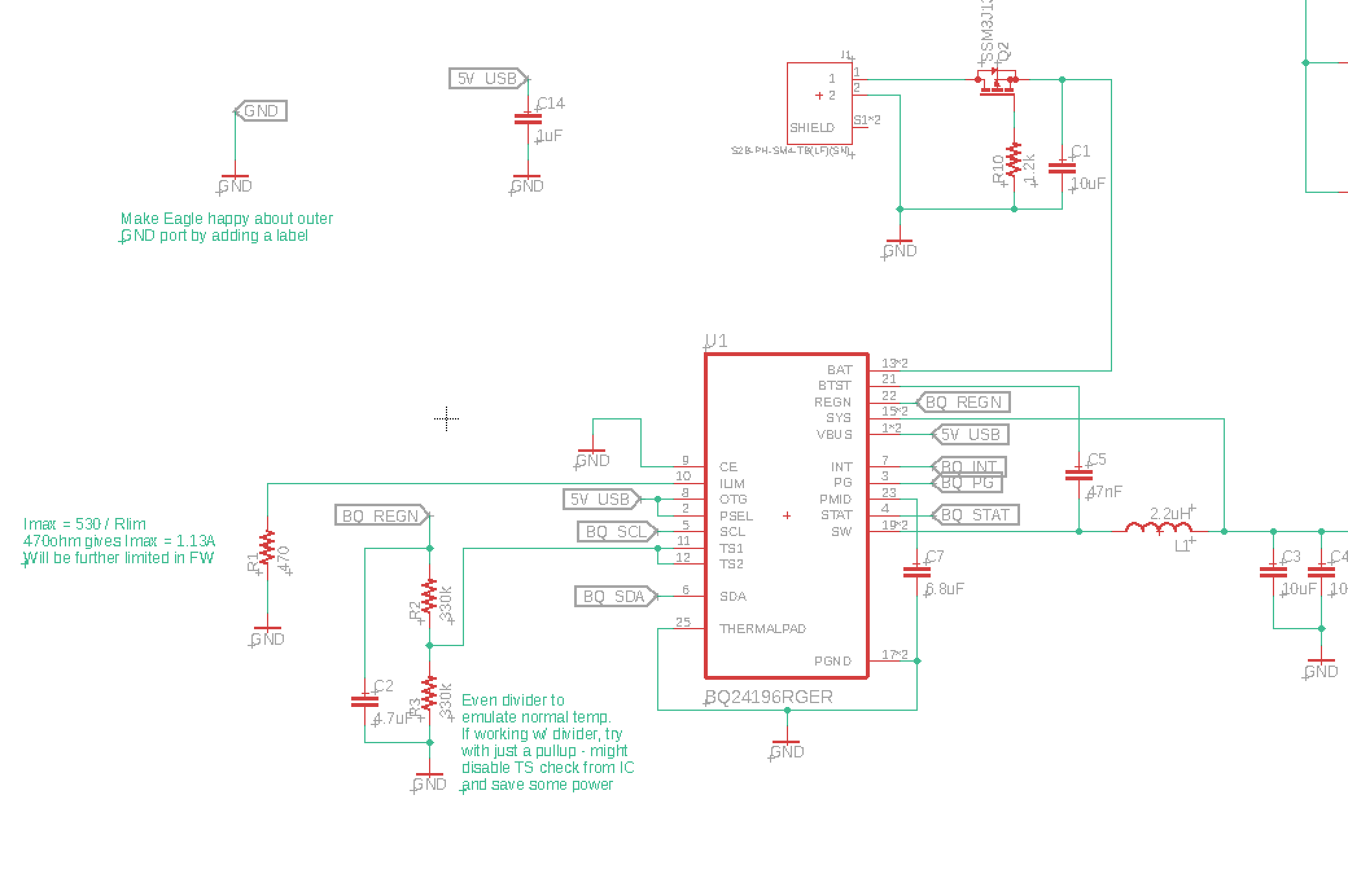
Zoomed-in view of the BQ section of the power schematic
The biggest unknown in the whole design for me was the battery charger chip from TI, the BQ24196. I had worked with a couple of them by this point, ranging from interacting with a driver someone else had already written to adding a couple of register tweaks for another. I had never designed or laid out the actual circuit around a chip but figured with the datasheet I couldn’t mess it up too badly (wrong).
I created the schematic matching the datasheet almost exactly. I subbed in a resistor divider to replace the battery thermistor since the inexpensive small LiPo batteries that I had did not have one in them. I also configured the OTG and PSEL pins to cap the max current at a higher value along with adjusting the ILIM current limiting resistor to give a max of 1.13A which I could then limit further in firmware.
In the rev. 3 schematic, I left out a very important capacitor in between BTST and SW which resulted in a couple of weeks of wasted debugging on why my output voltage would be fine with a battery but less than a volt with just 5V. That capacitor was the main impetus for rev. 3.1.
Similar to the FT232 chip, the BQ had two open-drain pins that indicated power good (PG) and status (STAT). I added two LEDs for easy state indication, but they’re mostly unnecessary and can be removed down the line for power savings.
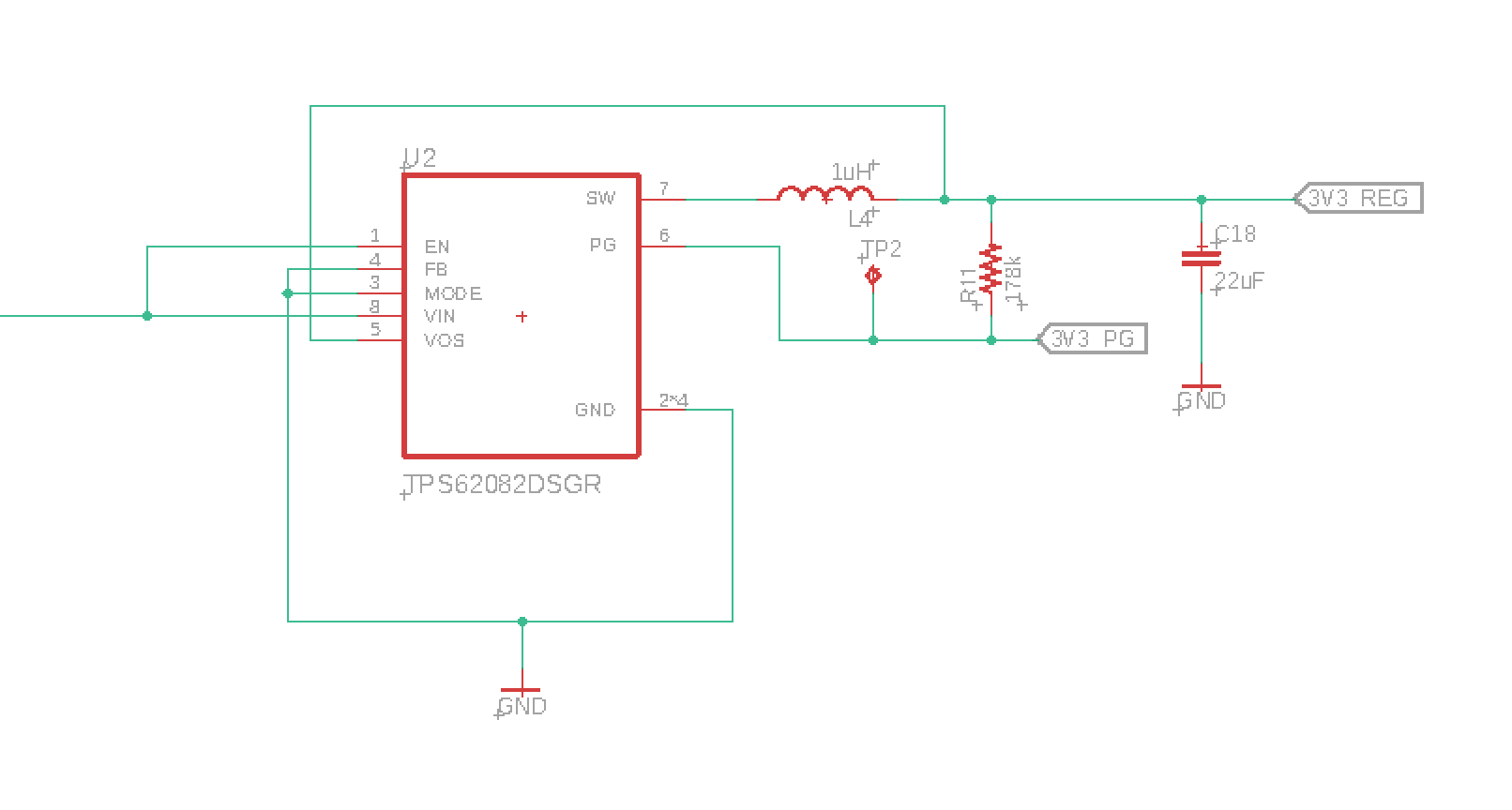
Zoomed-in view of the TPS section of the power schematic
The output of the BQ24196 charger fed into a 3.3V output buck regulator. This was a simple device (or so I thought) intended to regulate the ~3.4-4.2V output from the battery charging subcircuit to a clean 3.3V to power the remainder of the circuit. I chose a switching buck regulator to minimize quiescent current and wasted power. It would have to always be on to power the ESP32, so I wanted as minimal power loss as possible when on battery power.
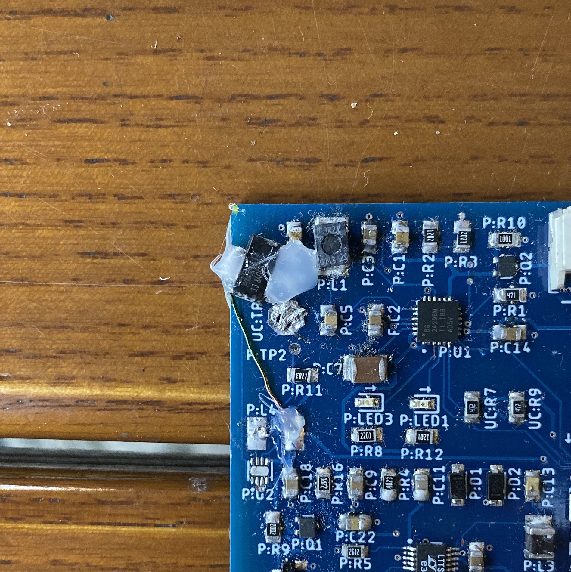
It's hard to see through the hot glue, but the AM1117 lined up conveniently with the BQ output and the large ground test point. The top Vin pin is connected to the output cap from the BQ, the bottom ground pin is connected to the test point, and Vout is connected to the remainder of the circuit with the green enamel wire.
Unfortunately, this choice also bit me. I ran into issues where the chip, which could supposedly support up to 1.2A of current draw, would show a full voltage dropout at anything over 200mA. I couldn’t find an answer to this after consulting with many different people and even asking on the TI e2e forums. I ended up desoldering an AM1117 3.3V LDO from an ESP32 dev board and bodging that on instead. The power draw is bad but for development at this point it gets the job done.
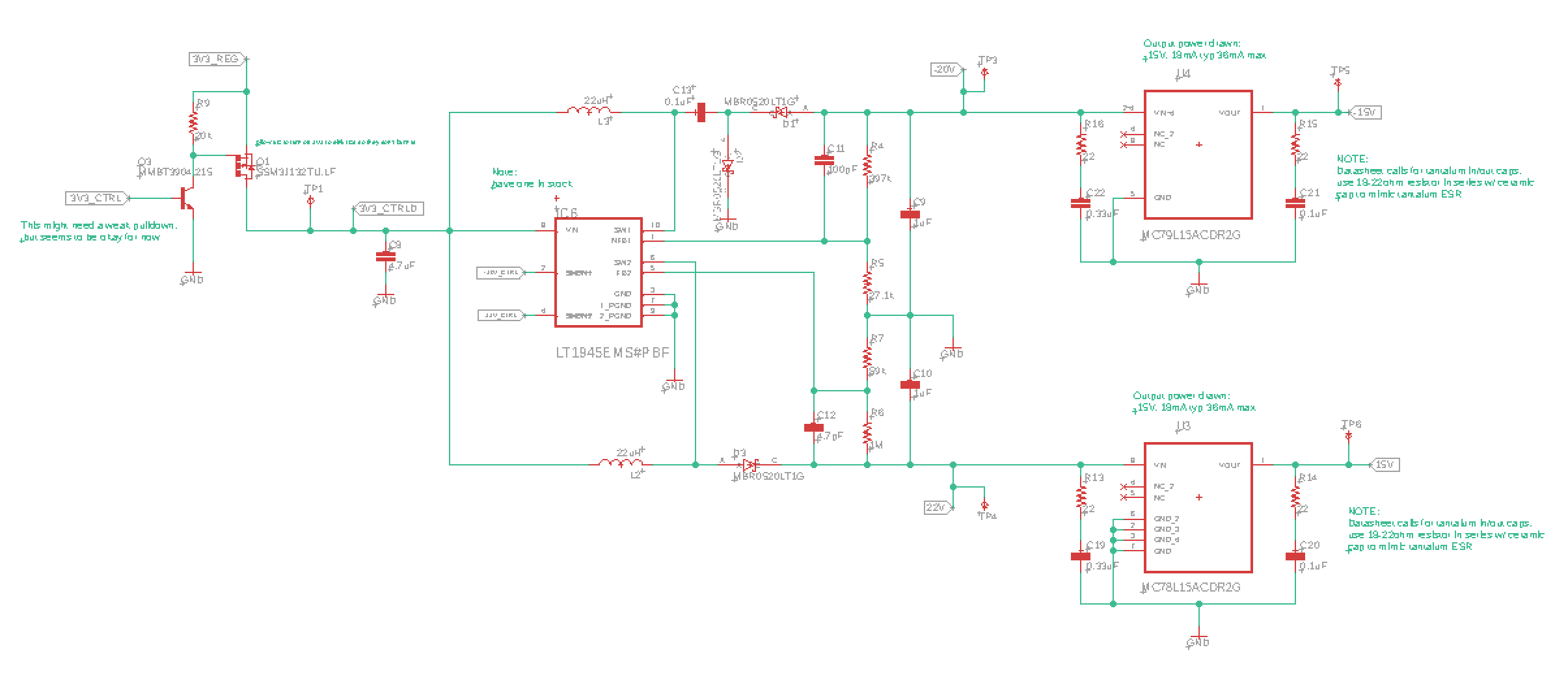
Zoomed-in view of the e-ink boost and linear regulator section of the power schematic
The remainder of the power circuit was pulled almost identically from the e-ink breakout board I already designed. It used an (expensive!) buck-boost switching regulator to boost the 3.3V up to 22V and -20V. These voltages fed into the e-ink connector and were also regulated to +/-15V for other e-ink inputs.
e-ink Driver Hardware

As I mentioned in the Power section above, the e-ink schematic was almost an exact copy and paste from the breakout board design. It involved a shift and store register, a fine-pitch 39 pin FPC connector, and an op-amp to feed the data correctly into the screen. More details on that integration can be found in the e-ink driver board post linked above.
I switched a few of the GPIO around to better fit in my design, but that was fixed with a couple of simple changes in firmware.
Microcontroller

The logic of the base microcontroller schematic stayed the same for the most part. I shuffled some pins around to add two I2C lines to communicate with the BQ chip. The WROVER version of the ESP32, which is the one needed by the epdiy open-source e-ink driver due to the extra RAM, has a couple of extra pins marked as NC compared to the WROOM as well. I simplified the button debounce design since it was less necessary with the auto-programming, and scrapped all but the JTAG and UART header breakouts just in case the USB programming didn’t work.
One downside of the epdiy driver is the number of pins it takes up. After the driver, the BQ I2C lines, and some input-only signals, the only R/W GPIO I have remaining to use is IO0, which I’d prefer not to touch if I can avoid it due to its importance in the bootloader sequence. There are a few extra read-only pins available, but that doesn’t help me.
Due to this, I had to repurpose each of the hardware-tied JTAG pins for application-specific functions. That means that I can’t run this board normally and debug over JTAG at the same time. I’ll have to implement a separate mode, but then I’m unable to drive the e-ink display or communicate with the BQ over I2C.
One of the main pieces of functionality earmarked for rev. 4 (if I ever do it) would be to use an I2C-driver IO expander to offload some of the epdiy driver pins and open back up the JTAG GPIO for programming and debugging.
Assembly and Bringup
Trying to bringup this board took probably around seven years off my life. All it was was problem after problem, concentrated mostly around the power subsection of the board but not entirely. Each build I did, one for rev. 3 and one for rev. 3.1, I built two boards to help rule out issues from assembly compared to design. It helped, but not entirely.
The first thing I ran into was the proper behavior of the BQ charger IC. It would output the expected voltage just fine when the battery was plugged in whether or not USB power was connected. Running just off of USB, however, showed only around 0.6V at its output. This seemed very weird, and I couldn’t figure out if there were register settings I needed to properly set to get VBUS-only power. The TI BQ series only comes in a VQFN package, so I was stuck trying to look for shorts or bad solder joints underneath this tiny IC with no microscope.
I found the first issue when re-reading the suggested design in the datasheet for what was probably the 70th time. I was missing a small 47nF cap between the BTST pin and SW output and had them shorted together instead. Unfortunately (as I’ve now learned is bad practice), I had connected the pads with a direct tiny trace between them since they were side-by-side, so I couldn’t cut it to bodge a capacitor in there. That was the first reason for rev 3.1.
The next issue I was running into was repeated brownouts of the ESP32 from the 3.3V buck regulator. It only happened when the Spot Check firmware was running, not when some simple espressif example code was flashed. I figured something was pulling a ton of current and causing the voltage from the TPS regulator to droop, but when I powered the 3.3V bus with my benchtop power supply, it only ever showed current spikes up into the high 200mA, and the TPS is rated for up to 1.2A.
I verified the output of the TPS was the problem, as a scope probe on the output pin showed a swift plummet down to about 0.9V at the time of brownout, where it stayed. Because of the BQ woes, I bypassed it entirely and bodged a wire straight from the 5V USB power to the TPS input. I confirmed this didn’t waver at all when the output died.
At the suggestion of some helpful folks, I hooked up a little test circuit to the output of the buck regulator to simulate current draw. I wired its output through a small resistor, then a pushbutton, then to ground. As I decreased the resistor size, I pinpointed exactly where the voltage output started to sag when a load current was pulled from the regulator.
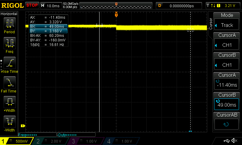
TPS regulator output with 183mA current load
The above scope shot shows a tiny perturbation in the output of the regulator when its load went from zero mA to around 180mA, courtesy of an 18-ohm resistor.

15 ohm load producing 220mA in current

12 ohm load producing 275mA in current
As I continued to drop the load and increase the current, the drop off of the regulator grew more and more severe. At only 275mA, it fell to less than a volt. That is not the expected behavior as described in the datasheet, which shows it should be able to take a jump up to 1A and recover back to its normal output voltage in less than 50uS.
I still haven’t solved this problem. I got a lot of help from others diagnosing it, and posted on the TI e2e forums as well but haven’t had time to follow up there. I worked around it by stealing an AM1117 3.3V linear regulator from a dev board and shoving it in the circuit in place of the buck regulator, which worked just fine.
Thankfully the subcircuit for boosting and regulating the different higher voltage rails, along with the e-ink data lines from the shift register, worked great. As it should, since I’ve already proven it out with the breakout board project, but I definitely wasn’t confident in it after the amount of pain that went into debugging the BQ and TPS.
Overall, I’ve proven out everything in the board design and it’s functioning as expected except for the 3.3V buck regulator. Since I’ve hacked it with the larger linear regulator to get it working the hardware is fully functional.
Next steps
Going forward, all changes for this revision will be in firmware and Typescript backend API. My two main decisions are:
- how should the forecast and general information be displayed on the screen
- how should I render the content.
The first point arises due to the fact that I have so much real estate to display text and even graphics now. Where the LED strips were extremely limited in their available horizontal space, I can use as large or small of a font as I want on the screen. That means I don’t need any user interaction at all and have the space to show the weather and general conditions like before, while also displaying the upcoming surf forecast information without having to rely on a user button press and scrolling text.
There’s room for other, non-surf-related information as well. I can set up the API to connect to theoretically any other external-facing service like my calendar, news, sports, etc. I think a longer-range goal would be to give the user the choice of setting different portions of the screen to pre-determined blocks. So there could be a surf forecast block in the upper right, news or Twitter in the bottom right, and the left side could be their calendar. It would give flexibility in the choice and arrangement of information.
That leads to the second point of how to render the content. The epdiy library exposes simple functions like drawing text and shapes at specific coordinates. While this is nice for on-device handling of info, it’s much more difficult to make the UI and UX nice. Since the epdiy library can render images, a second option is to build the entire image of data within the backend API, and serve that to the device whenever it requests updates. That way the Spot Check firmware can be fully blind to the actual data it’s displaying, and just request and display whatever image it gets.
The full-screen re-render takes more power than just refreshing small parts of the screen, but I’m willing to be that power consumption is dwarfed by the power draw from sending a wifi request and downloading an image response.
Even though it was an enormous pain in the ass to get working and there are many more small hardware changes I’d make if I spun another revision, I consider the jump from rev. 2 to rev 3.X a success overall.