Spot Check pt. II
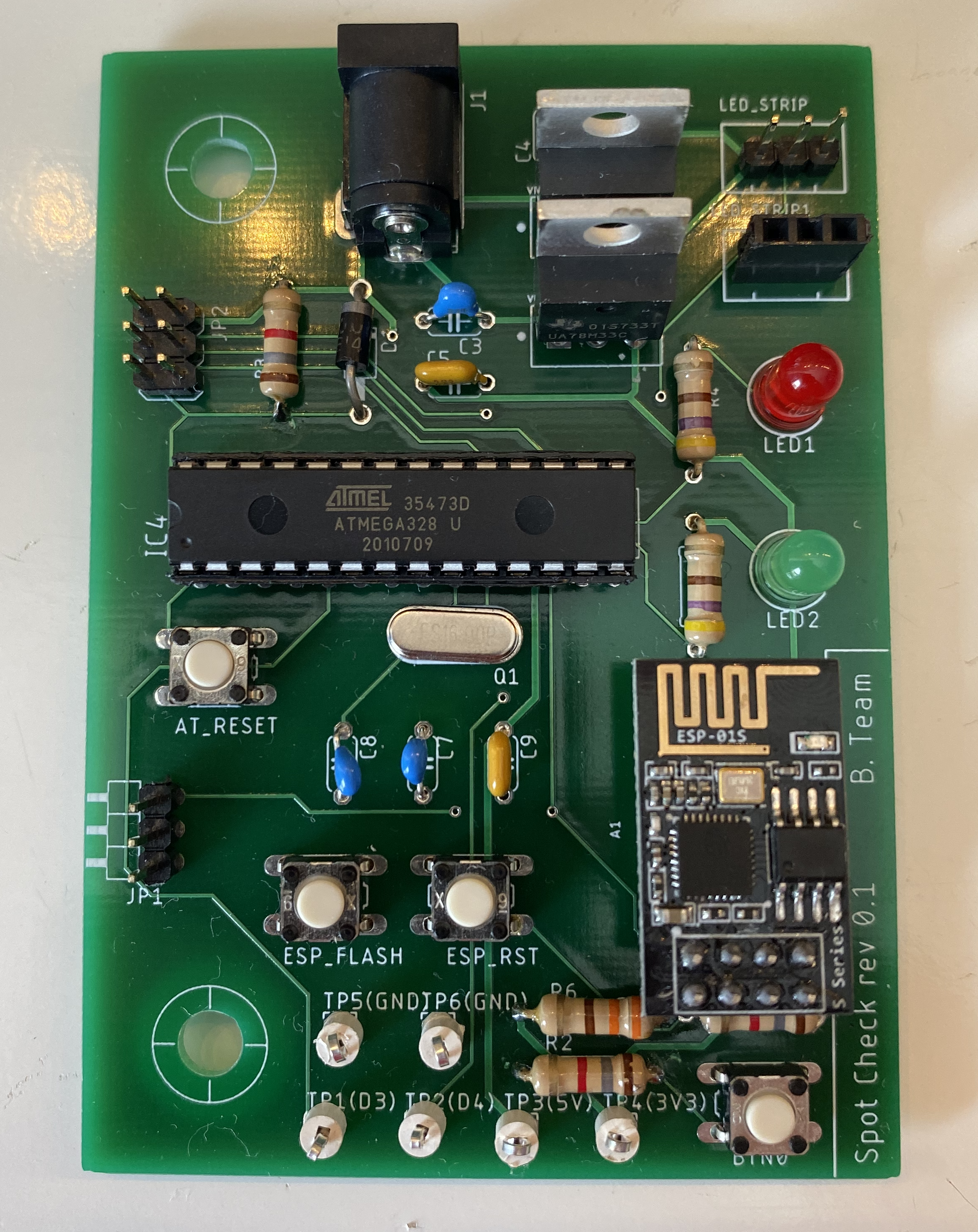
In the first portion of this project, I breadboarded out the prototype to ensure everything would work end-to-end. This included linking up two full-size dev boards along with the LED strips and passive components. The next step was to design a custom PCB that could encompass the entire system on a single board.
Schematic and component selection
My approach to the schematic was split up into multiple large chunks. These were the logical separations within an architectural diagram of the system: power, the ESP-01, the ATMega chip, and the connection to the LED strips.
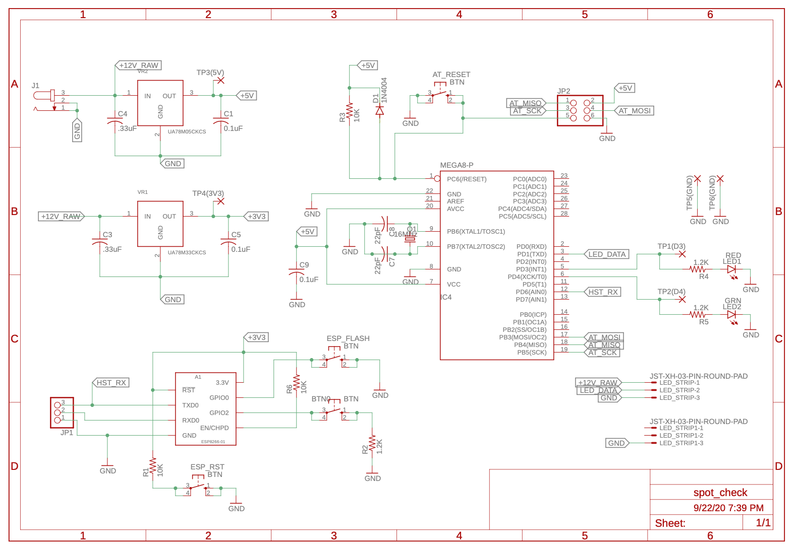
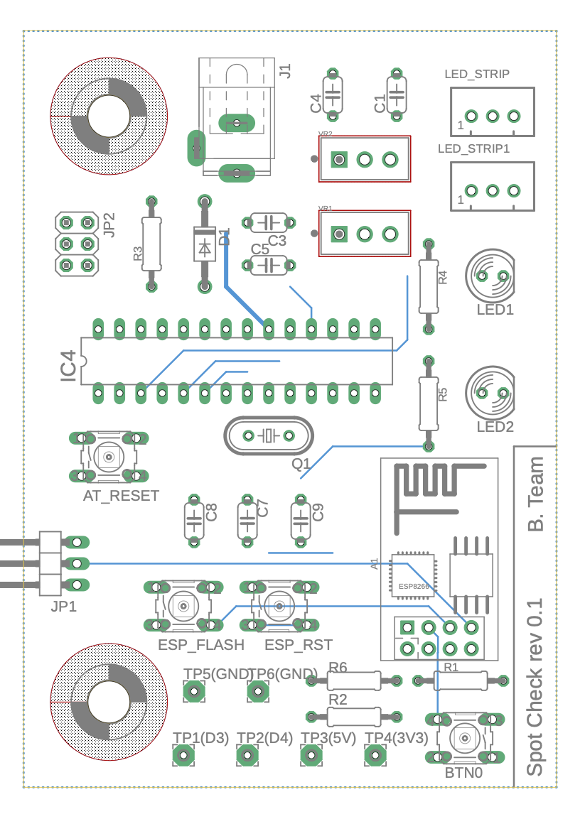
Right-click and open in new window to zoom in
In my first pass at the schematic, I didn’t worry too much about getting the exact right components that would be the final parts. Eagle has a massive library of parts, and those are still only a small subset of the custom ones on the internet. I made sure that I was choosing through-hole components that seems roughly the correct size, but beyond that, I wasn’t too concerned about the footprints yet. After finishing the entire thing, I returned to each piece to ensure that the size matched what I measured for my existing parts and replaced those that didn’t fit.
Power
I needed three total voltage levels: 12V (with decent current too) for the LED strips, 5V for the ATMega, and 3.3V for the ESP-01.
I had a 12V @ 2A power block lying around, so I didn’t feel the need to regulate the power I fed to the LEDs. Ideally, I would have another regulator that allows the use of 12V+ blocks up to a certain current and voltage level, but I wasn’t too concerned about the noisy supply for this iteration.
My initial plan for the 5V and 3.3V levels was to first knock the 12V down to 5V, use that to power the ATMega, then knock the 5V down to 3.3V. With the cheap linear regulators I was looking at, however, there was too much of a dropout voltage to do that (the 3.3V regulator needed at minimum 5.3V at its input). I could have gone with an LDO or a switching regulator, but I didn’t want to pay more and have to dig too much deeper (read: I’m lazy).
Instead, I dropped 12V down to each level separately. The regulators I chose had plenty of ceiling in terms of voltage max to handle this. I also ensured they could handle an appropriate amount of current. Since I’m powering the LEDs through the 12V separately, I knew the ATMega would never draw that much when running max three data pins.
One thing I realized quickly was that I should have done a little more math with the 12V -> 3.3V conversion. Since the regulator itself is dropping 8.7V (12V - 3.3V), it would be dissipating close to 1W of power (8.7V * 150mA). I didn’t measure the full current draw of the ESP-01, but from what I found online it can easily draw in the 200mA range when transmitting or receiving data. It’s not really a problem since the regulator is still rated for plenty more current, but it does get fairly hot to the touch after operating for a while.
The regulator schematic is designed with bypass capacitor values pulled from the datasheet. I also routed two test points off of each output to be able to easily test if they were outputting proper values.
ESP-01
The ESP-01 block of the schematic is very simple, and I designed it based almost directly on online schematics for programming the ESP on a breadboard.
The ESP board itself already has all of the resistance and capacitance it needs to run. The few basics I had to add were to enable programming the board (duh), serial output to talk to the ATMega, and a button GPIO input.
It takes 3.3V for power and the enable pin for it to run. The reset is active low, so it also takes 3.3V with a button to function as a pull-down to ground. GPIO0 is a dual-purpose pin. It can be used as a regular GPIO pin but is also necessary for the flash process. It needs to be held low for the entirety of programming, so it also gets a pulldown button.
I actually made a mistake with the reset button. The way it’s wired, it will never properly pull the reset input to ground since the resistor dropping the full 3.3V is below the chip input. I fixed this on the board by soldering a jumper wire between the reset pin and the bottom of the resistor. I was a little surprised this didn’t make the board go boom since I’m technically shorting 3.3V straight to ground, but I guess the regulator has enough built-in protection to prevent the current rush for the short time the button is held.
Since the ESP-01 only breaks out a single set of the serial pins (the ESP8266 has 3 UART ports), I had to share the serial transmit between the programming RX pin and the ATMega’s input pin. This wasn’t an issue since the ATMega parsing code for the data fed in ensures it only handles “real” data with the use of some special character identifiers.
I decided to use the input power for programming instead of also pulling it from the programmer input since I didn’t want to have to deal with the potential voltage differences and backrush current shorting the USB port of my laptop. It’s not a hassle, it just means I need to use the main power input when programming the chip instead of being able to rely on the serial input.
ATMega
The ATMega section of the schematic was the most complicated piece, and I cobbled it together from a few different sources online. The Arduino UNO schematic was my main source of information. I knew I didn’t need to worry about the programming chip or its setup since I could use my existing Arduino dev board to program straight to this ATMega’s ICSP connections.
The crystal was one piece I was a little iffy on since I couldn’t find clear information on whether I just needed a crystal or a powered resonator. I pulled the ICSP programming section for the chip straight from the Arduino schematic. I have yet to try it out, since I’ve just been pulling the chip out of the DIP socket to program it in the Arduino board itself, and then placing it back in the PCB. The 22pF bypass caps were chosen based on the datasheet, and they also match the Arduino schematic.
The only necessary GPIO for me to break out were the input pin to receive the ESP serial data and the output pin for the LED strips. I also broke two additional pins out both to their own LED and test point. These don’t serve a specific purpose but will help with any debugging I need to do since I don’t have a scope to throw on them. It also serves a nice purpose if I want to display some system info from the LEDs down the line.
LED strips
The final piece was the connection to the LED strips. The main connector supplies power, data, and a ground pin. I broke a second one out that was fully grounded because I found that the strips tended to flicker and have some phantom LEDs on when the furthest end was left floating.
The strips themselves have an interesting clip-in connector that I couldn’t find an exact match for online. The closest I got was a specific JST connector, but it didn’t fit right. I ended up just soldering a section of three male pins in the main connector and an identical female connector in the second spot. It’s not perfect but it’s somewhat sturdy and gets the job done for now.
Board layout
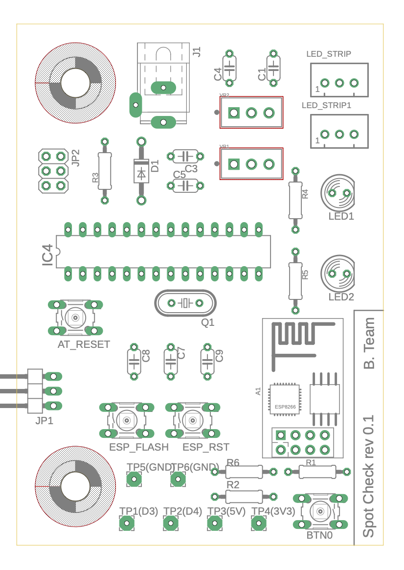
Full view of the board layout and routed traces
I had zero constraints when it came to board size and connector placement, so it was a relatively simple layout and route. I kept everything spaced out pretty far to keep the routing as simple and clean as possible. There’s room for improvement still, but for a 0.1 alpha, I’m okay with how it turned out.
I went a bit above the default minimums from my board manufacturer since I had the space and didn’t feel like having to worry about trace width. The power traces are 20mil and the data lines are 7mil
I grouped the voltage regulators close to the power block, and the LED connector with 12v next to them. All bypass capacitors are placed as close to their component counterparts as possible, and the ATMega crystal is similarly grouped with the chip.
Since I had so much space to work with I never considered more than a 2-layer board. Instead of going my normal route of all vertical on one layer and all horizontal on another, I tried to keep all traces on the top layer to leave the bottom for as consistent of a ground pour as possible. It worked out for the most part, but I think my layout could have been a bit better to group everything up top.
I grouped the ATMega and its components above the ESP, which in hindsight might have not been the completely correct call. I think splitting the board vertically down the middle and having ESP on the left and ATMega on the right would have let me send the central power down the middle and not have to deal with any vias and bottom traces at all.
Since both 5V and 3.3V were only used on a few pins, I didn’t feel the need to do power pours on the top half. I probably could have done another ground plane up top, but that seemed overkill for this simple of a board.
I grouped all of the test points at the bottom and attempted to keep all of the buttons somewhat localized to their chip/function. This led to some longer traces and was purely aesthetic, but makes it look much better than scattering things all over the place. I also added two mount holes on the corners because why not. I doubt I’ll need them for this version of the board but I’d rather have them and not need them than vice versa.
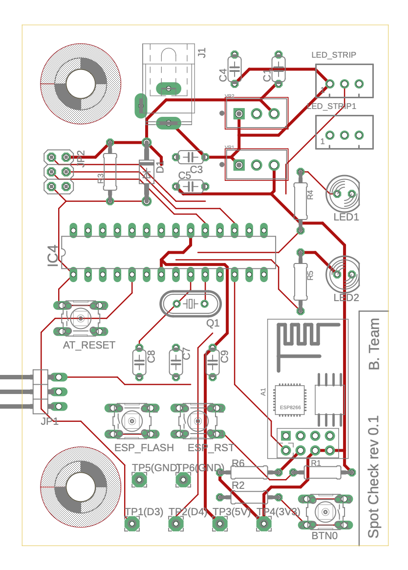
Traces on top layer of PCB
Traces on bottom layer (ground pour not shown)
Board assembly and debugging
After soldering all of the components on, I powered up the board and started to test it out. The highlights of the process went as follows:
Power
- Check the two voltage test points and find 0V on both - get very irritated until I realize that the multimeter fuse was blown
- After plugging in the power for a minute, the board still hasn’t blown up - good start
ESP-01
- ESP gave its normal blue LED flashes on power which is a good sign
- ESP reset button doesn’t work, tested with multimeter and never gets pulled low
- Getting serial gibberish at first from ESP
- Pull ESP from the board and hook it straight up to the serial programmer connected to USB, verify baud rates and transmission
- Reconnect to board, double-check connections, somehow correctly printing serially to monitor
- Short reset manually from chip to ground with a jumper and verify it works from output resetting
- Test flashing process while in-board with manual reset and flash button held, works as expected
ATMega
- Power going to LED strips correctly but no text
- One or two phantom LEDs lit on strips even with both ends grounded
- Realize I can’t monitor ATMega serial port since I only broke out ICSP not UART too (facepalm)
- Test on-board LEDs by hardcoding them on, still nothing
- Narrow it down to a clock issue since no GPIO is changing even when probing the actual chip pins
- Look at schematic, notice picture below, double facepalm
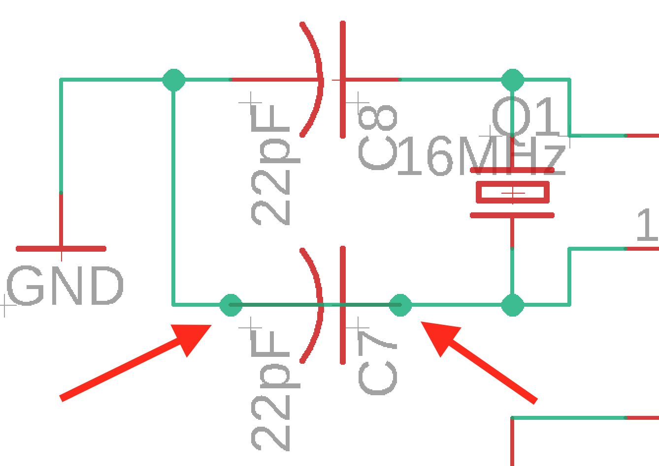
One of the bypass caps for the crystal being sneakily shorted to ground
- Realize I can’t just cut traces because the ground plane is fully connected to all three pins
- Use a razor and chop out all three pins that are grounded and wire them together
- Verify they’re all properly isolated by measuring impedance to ground. When they’re all floating just like the other side of the crystal, they’re good
- Basic code to turn on on-board LEDs runs as expected on PCB
- Switch ATMega code to hardcode print a value to LED strips
LED strips
- See tiny scratch in trace connecting ATMega LED data to strips from a slip when chopping out grounded crystal pins
- Manually connect ATMega pin straight to strip with jumper wire and it prints text
- Try to push solder into the crack of the cut trace, no go
- Solder another long jumper from IC socket pin to bottom of led strip pin
- Still doesn’t work even though wire has correct data, not passing it up through the pin somehow
- Accidentally short ATMega somehow, won’t program or work anywhere
- Order two new DIP ATMega chips
- Decide while I’m waiting to put together a second board to make the isolation of the 3 crystal pins cleaner
Second assembly
- Cutting traces for second PCB way smoother
- Cut the four small ground plane connections per-via instead of a full box, measured with a multimeter and all good
- Solder all components again, lower current-limiting resistors for reset pin so they’re closer to voltage expected by chip
ATMega take two
- Accidentally get ATMega328s instead of ATMega328Ps (note the
P) - Spend some time fiddling with the Arduino IDEs internal files to correctly burn a bootloader to the 328s
- Flash code to new chip, insert in PCB, promptly hear it pop and fry another chip
ATMega take three
- Order more chips, flash bootloaders, and work much more carefully with plugging/unplugging power since I think that’s what caused the blowouts
- Still stuck with crystal issues, switch it out for a known working one
- Again seeing the behavior with the LED data line where the signal is seen all the way up until the connector pins
- If I attach the LED strips directly to the board, the signal never makes its way to the LEDs
- If I remove just one pin from the LED connection and instead manually jump that by hand to the exact same pin on the PCB, it works
- Baffled at this point, but at least I know the board works (mostly) beginning to end
- My theory is that there’s either A) an issue with grouping power/ground/signal together so tightly and somethings getting interfered with or B) having fast signals returning to the same ground pour that power is using is messing something up
So overall at this point it “works”. After all of this effort and work, I’ve decided that this ESP-to-Arduino data transfer is just way too brittle, and I’ve been looking into ways to remove it. There exist ports of the FastLED and Neopixel LED strip libraries for use on ESP-32s, so I think I’m going to spend some time seeing how much work it would be to use that instead of the Arduino/ESP8266 combo. I plan on giving this library a shot to see what I can make happen. Very happy I went through this process even though I won’t use these boards - it was a lot of fun to get back into the EE side of things!