Spot Check pt. IV
firmware repo
node.js api repo
iOS app repo
Previous project updates:
After finishing the firmware and prototype enclosure described in the Spot Check pt. III post (linked above), my next step was to create a new revision of the custom PCB for this project.
Custom PCB instead of dev board
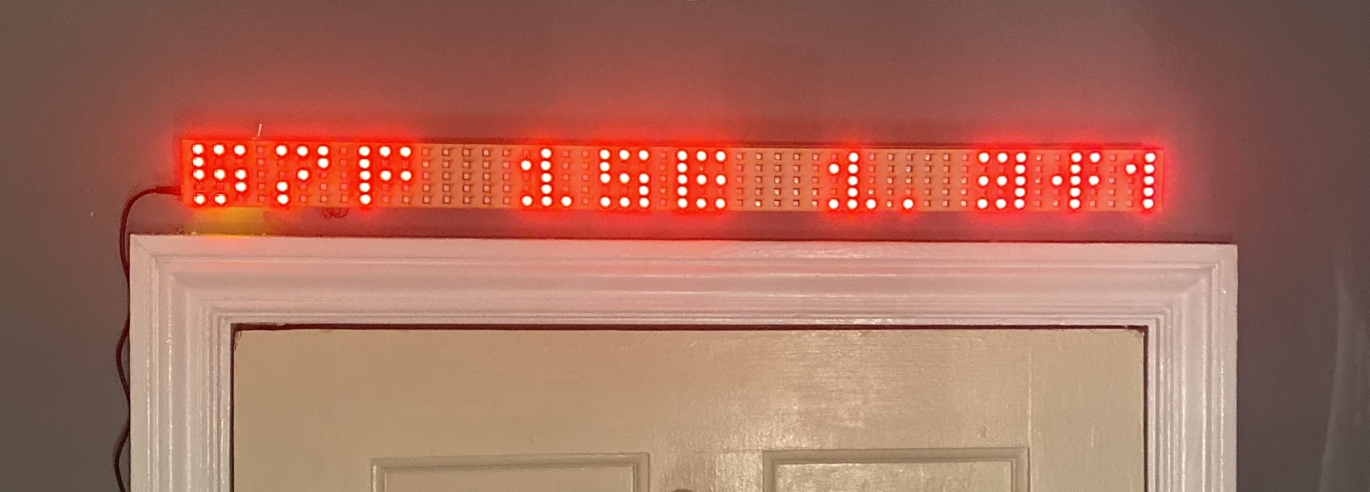
Considering I could run almost every peripheral I needed off the ESP-32 dev board GPIO, there wasn’t a pressing need for a new board. The one major reason why I felt it necessary was to be able to supply a safe amount of power to the LED strips. Since there was only ever ~30% of the LEDs lit at once time to display text, there hadn’t been an issue powering them from a laptop USB port and through the ESP-32 GPIO.
Just because something happens to work definitely does not mean it’s the right thing to do. Even though most laptops these days have USB ports rated to source way more power than required by the USB spec, I wanted to be on the safe and proper side in case there was ever a short or bug that caused them to pull a bunch of power. The GPIO on the ESP-32 are also only rated to source 150-200mA, so powering a set of LEDs that are capable of pulling 10s of amps from one of those pins is another terrible idea. I added a regular DC barrel jack to the board to use a 5V, 3A switching power supply that plugged into a wall outlet.
The second reason I wanted to create a new board was because I enjoy doing it! I don’t get to practice my EE knowledge as often as I do software or firmware, so if there’s any advantage to designing something custom that won’t take too long I jump at it. Without fail, I learn multiple new things every time I design a new schematic + board.
Schematic
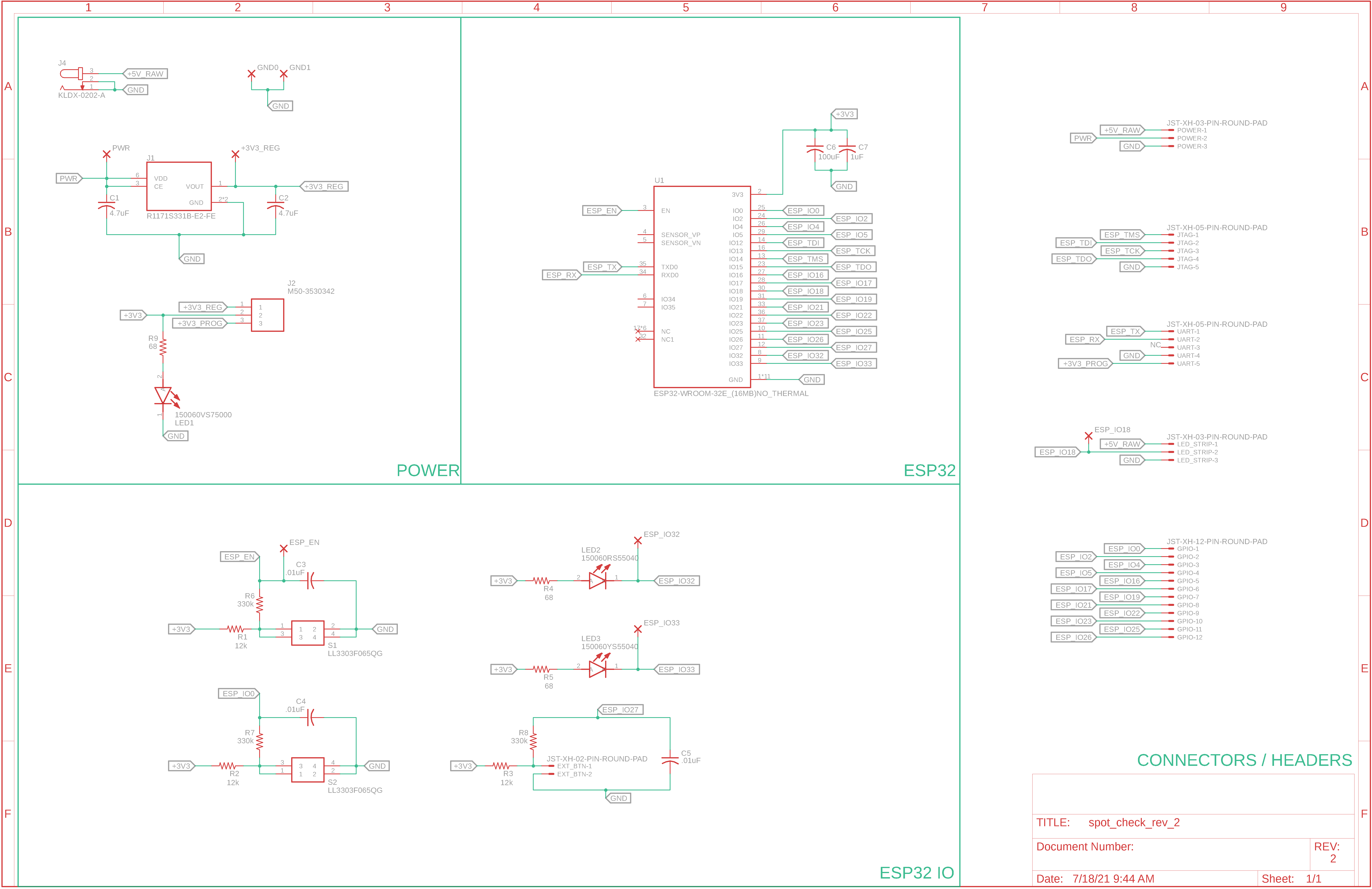
This design was so simple that I could fit every design block within a single schematic page.
Power
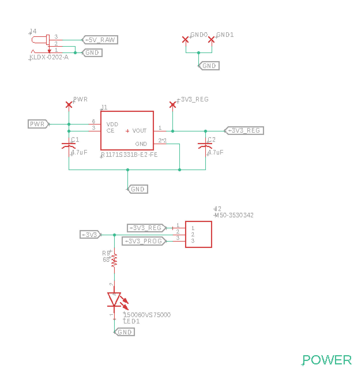
Like I mentioned previously, I chose to power the whole board from the 5V barrel jack input. The raw 5V signal was routed both to the power pin for the LED strips and into a 3 position header. I wired a toggle switch into the header location to use as the master on/off switch. I realized after assembly that I should have routed the output of the toggle switch to the LED strip’s power pin instead of the 5V straight from power since I effectively had no way to turn off the LED strip power. Since they save whatever was last programmed to them as long as they have power, this meant that they would remain on and displaying text after the ESP-32 was powered off.
I routed the 5V signal coming out of the toggle switch into a 3.3V fixed LDO to step the voltage down to the ESP-32’s level. However, instead of powering the ESP-32 directly off the 3.3V regulated output, I added another 3 position header on the line to be switched with a jumper. The other input to this header was the 3.3V line from the programming pins. This let me power the board with the programmer (since I was programming over serial, not USB) without having to power the board separately while flashing code to it. I chose this jumper configuration to give me the flexibility to power from either wall or programmer but not both, since I didn’t have any backpower protection. I could have used a Schottky diode on each power input but I didn’t want to add in even the minimal voltage drop that would come with it.
ESP-32
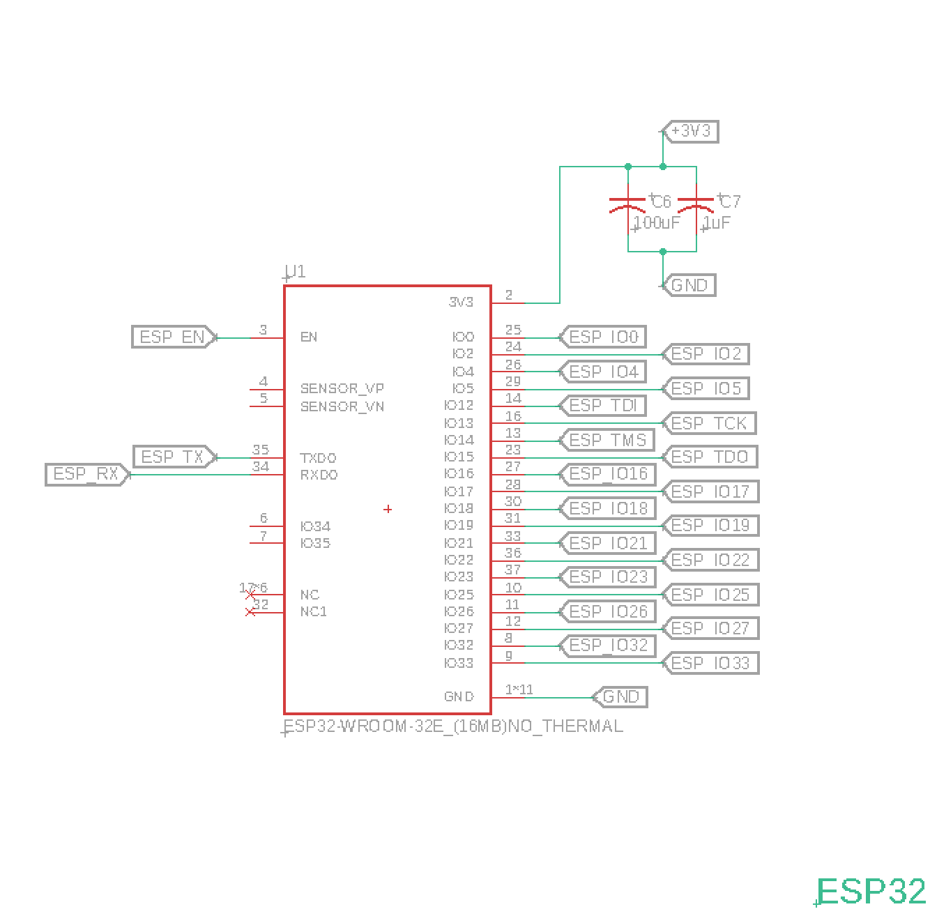
This is about as straightforward of a pinout as can be. The power pin is tied to 3.3V with a 100uF and 1uF capacitor across it (values recommended by ESP-32-WROOM datasheet). The enable and IO0 pins both come from the output of hardware buttons to enable reset and programming, TX and RX come from the programmer header, and every other GPIO besides two are broken out to header pins. In situations like this where PCB length isn’t restricted by the enclosure, I always try to break out as many potential pins as necessary just for the sake of being safe. You never know when another GPIO will come in handy, and for any pins I don’t need I simply won’t solder a header into that hole.
IO
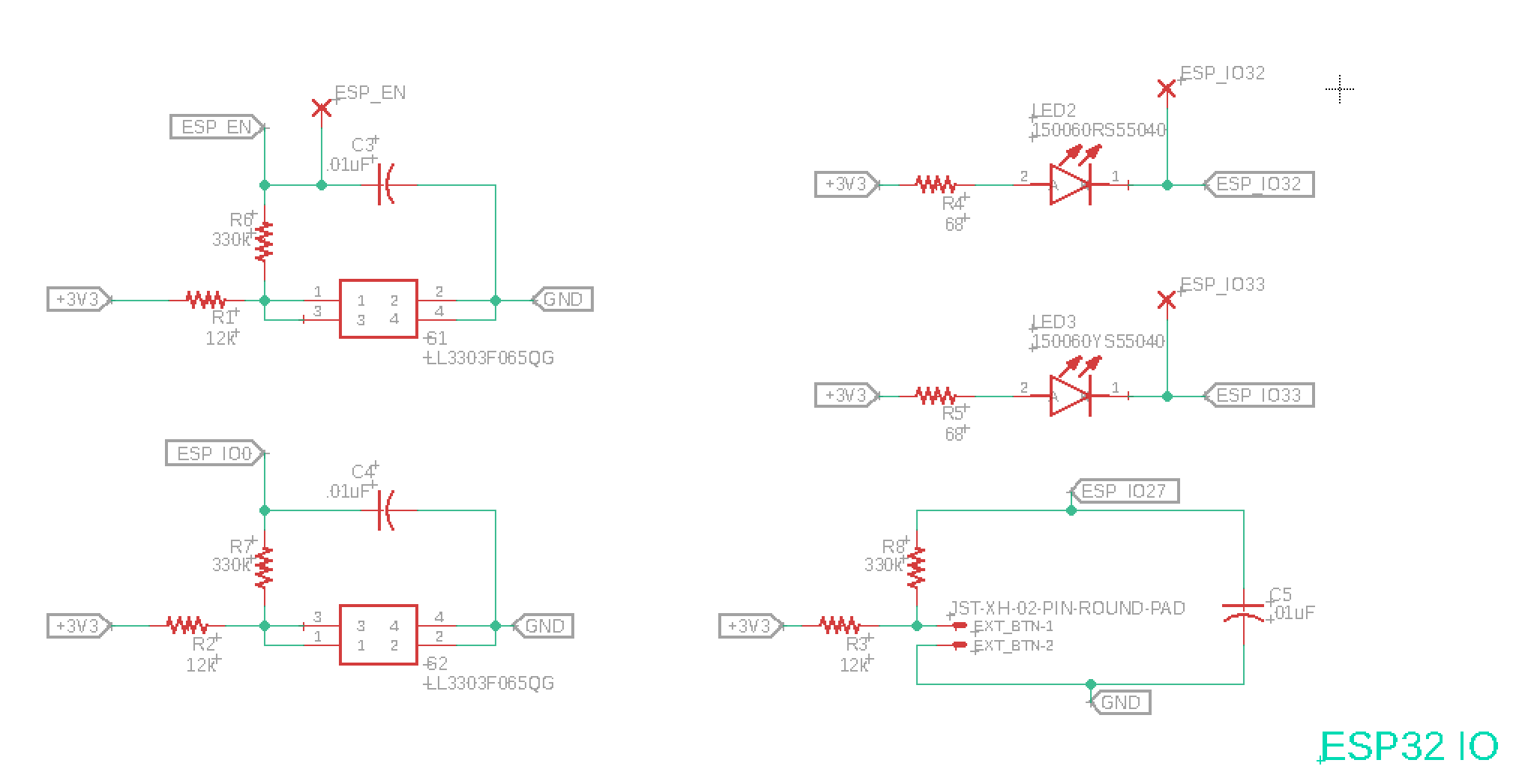
I added two buttons for programming and resetting the board. The ESP-32 requires its IO0 pin to be held low at boot to switch the bootloader into programming mode, and a button tied to ground is the easiest way to accomplish that for repeated use when developing firmware. The EN pin on the ESP-32 is weakly pulled up internally to maintain its active-high on-state when running, but I included an external pullup similar to the IO0 pin that will be pulled low and cut power to the internal voltage regulator when the button is pressed.
The third button in the bottom right of the above schematic image was routed to IO27 of the ESP-32 and served as the user input to activate the forecast display from the firmware. It uses two board drill-holes rather than an on-board button since I wired a large external pushbutton to the board from the edge of the enclosure.
Each button is debounced in firmware, but I also added a simple hardware RC debounce circuit. I chose values based on an expected settling time of roughly 20ms from the hardware bounces. I simulated both a button press and release in LTspice as seen in the screenshots below. Vi is the simulated input of a button being pressed and bouncing rapidly, Vo is the output voltage smoothed by the RC circuit.
Obviously button bounce is an intrinsically unknown value from hardware but the goal with the hardware debounce was to mitigate the effects of the bounce, not to remove it completely. The firmware could handle any remaining oscillations.
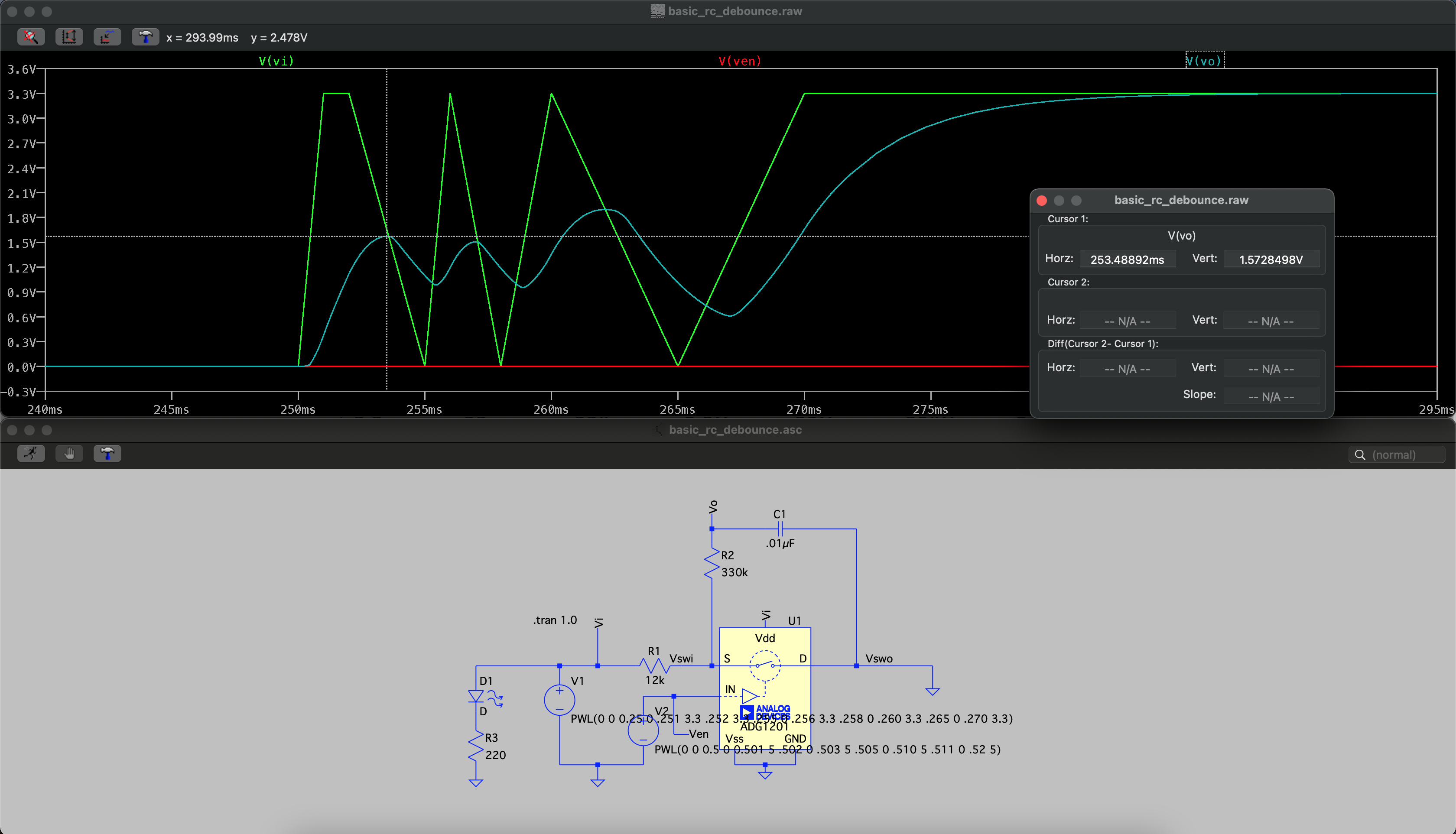
Simulation of a button press
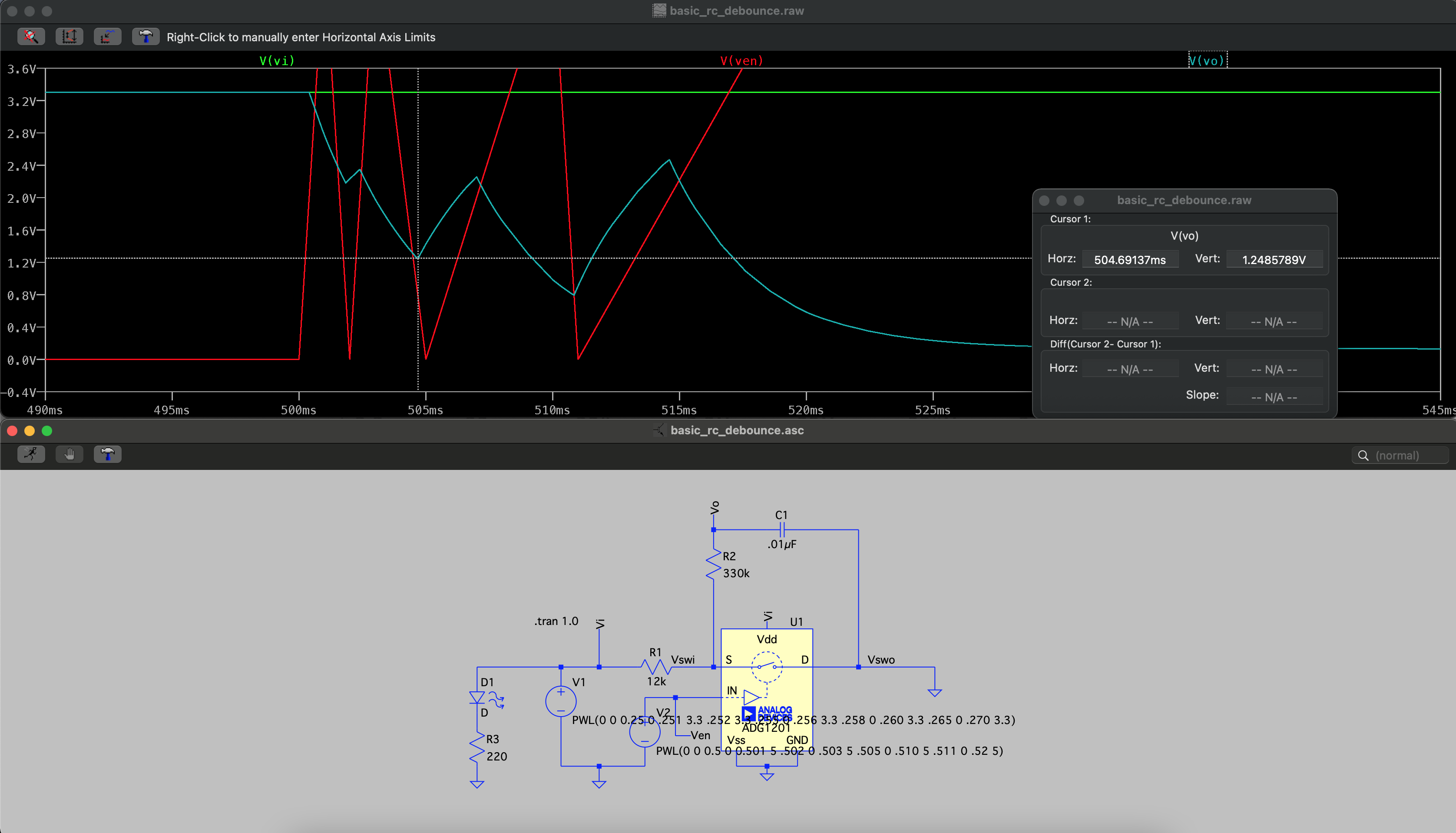
Simulation of a button release
The remaining two IO components were simple indicator LEDs tied to available GPIO on the ESP-32. I added them to serve as debugging output if necessary, to more easily indicate different state changes in firmware rather than having to measure voltage on a pin. Both signals are also routed to test points in case faster signal analysis is needed with a scope.
Through-hole connectors and headers
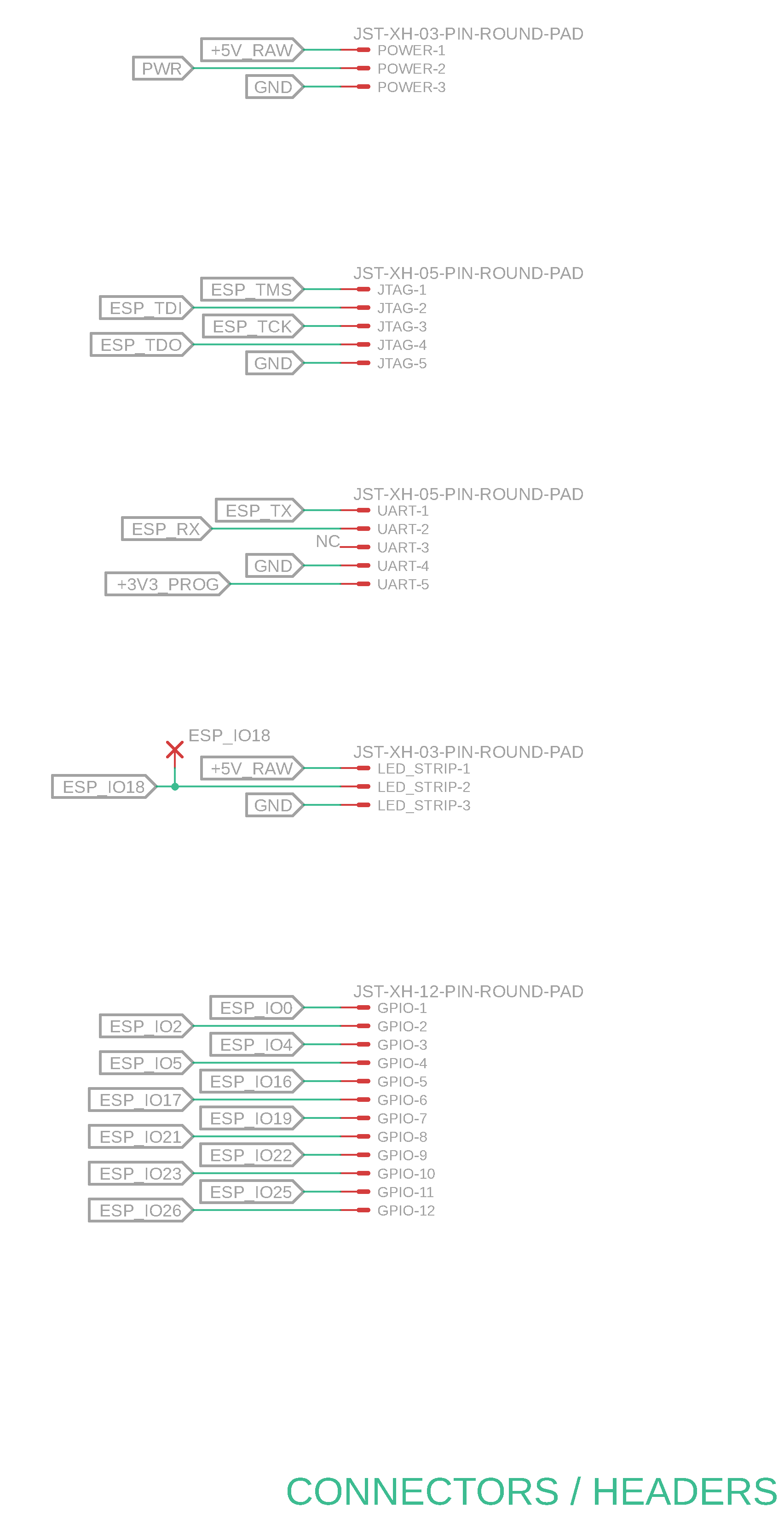
This section is included mostly for completeness’ sake to detail the entire schematic but is quite straightforward. A list of the purpose of each connecter grouping:
- POWER - the power toggle switch mentioned in the Power section above
- JTAG - a 5-pin header for debugging over JTAG tied to the ESP-32’s JTAG-specific pins
- UART - another 5-pin header for programming and outputting over a serial UART
- LED_STRIP - the 3-pin header for connected 5V power, ground, and the signal line from the ESP-32 to the LED strips
- GPIO - the remainder of the ESP-32 GPIO broken out into a long header line because I had the room on the board and why not
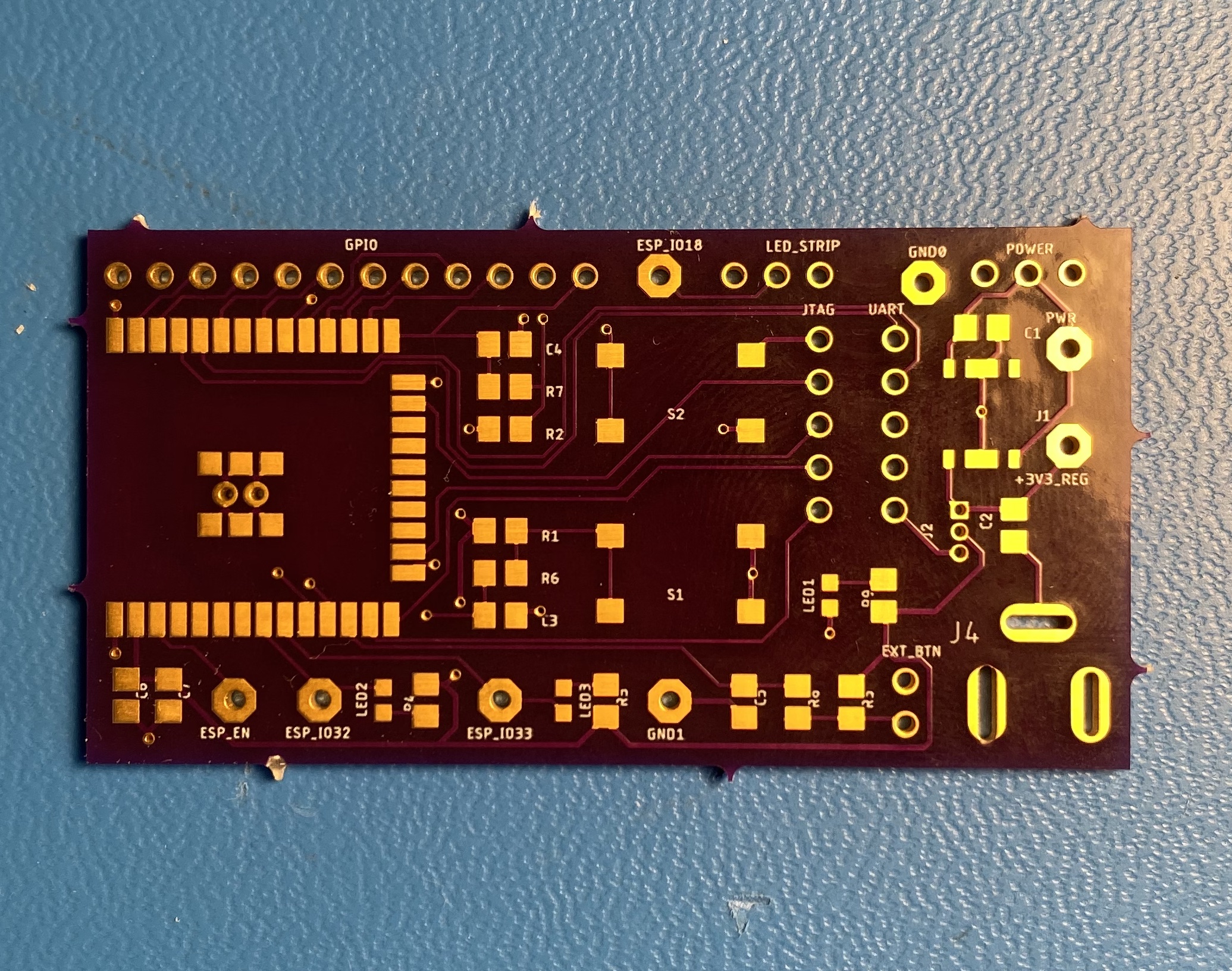
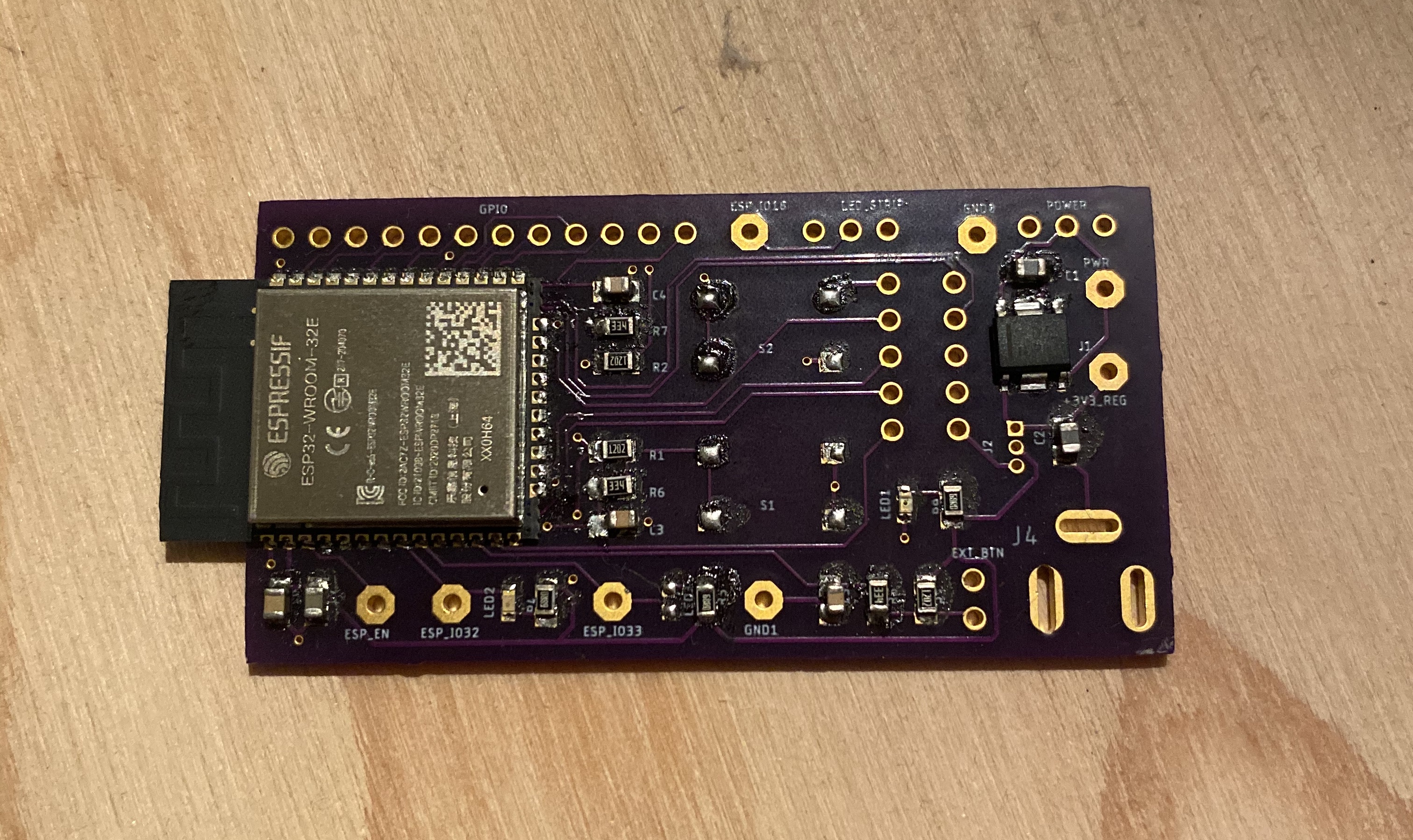
Board
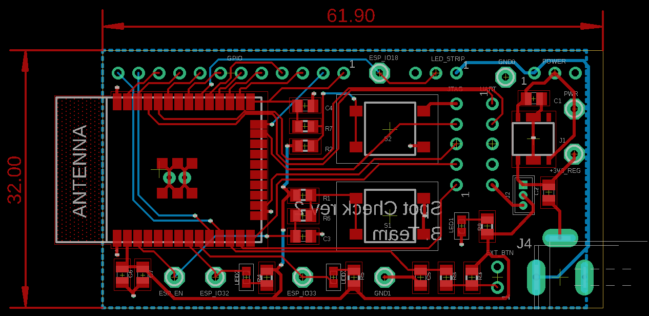
Component selection and layout
I went with a majority of SMT components for this design because I wanted the board to be able to fit comfortably in the relatively thin enclosure. The size ended up being almost identical to the ESP-32 dev board, but I was maximizing more for a clear and simple layout rather than minimal board area.
The two other main constraints besides board dimension were the ESP-32 PCB antenna and the DC barrel jack. The datasheet for the ESP-32 recommends hanging the antenna strip of the ESP-32 chip PCB off of the edge of the main PCB to minimize any RF interference. That meant I needed to use most of the full edge of one side of the board without adding any other components or headers there. It was fairly simple since the 3-sided pinout of the ESP-32 lends itself to an end-of-board location to be routed out from there.
The last constraint was that I needed the power connector hanging off the board enough to protrude through the enclosure side once mounted. I also needed to ensure that the board orientation was correct for the power jack to exit the enclosure on the side, preferably closer to one of the corners of the side rather than the center.
Once I had the major components set, it was a fairly simple and logical layout from there. Bypass capacitors were all placed close to their respective ICs, the buttons were aligned next to each other in the center of the board with their debounce passives, and the 5V header for the LED strips was positioned close to the power input to avoid having a large trace power line throughout the board.
Trace routing
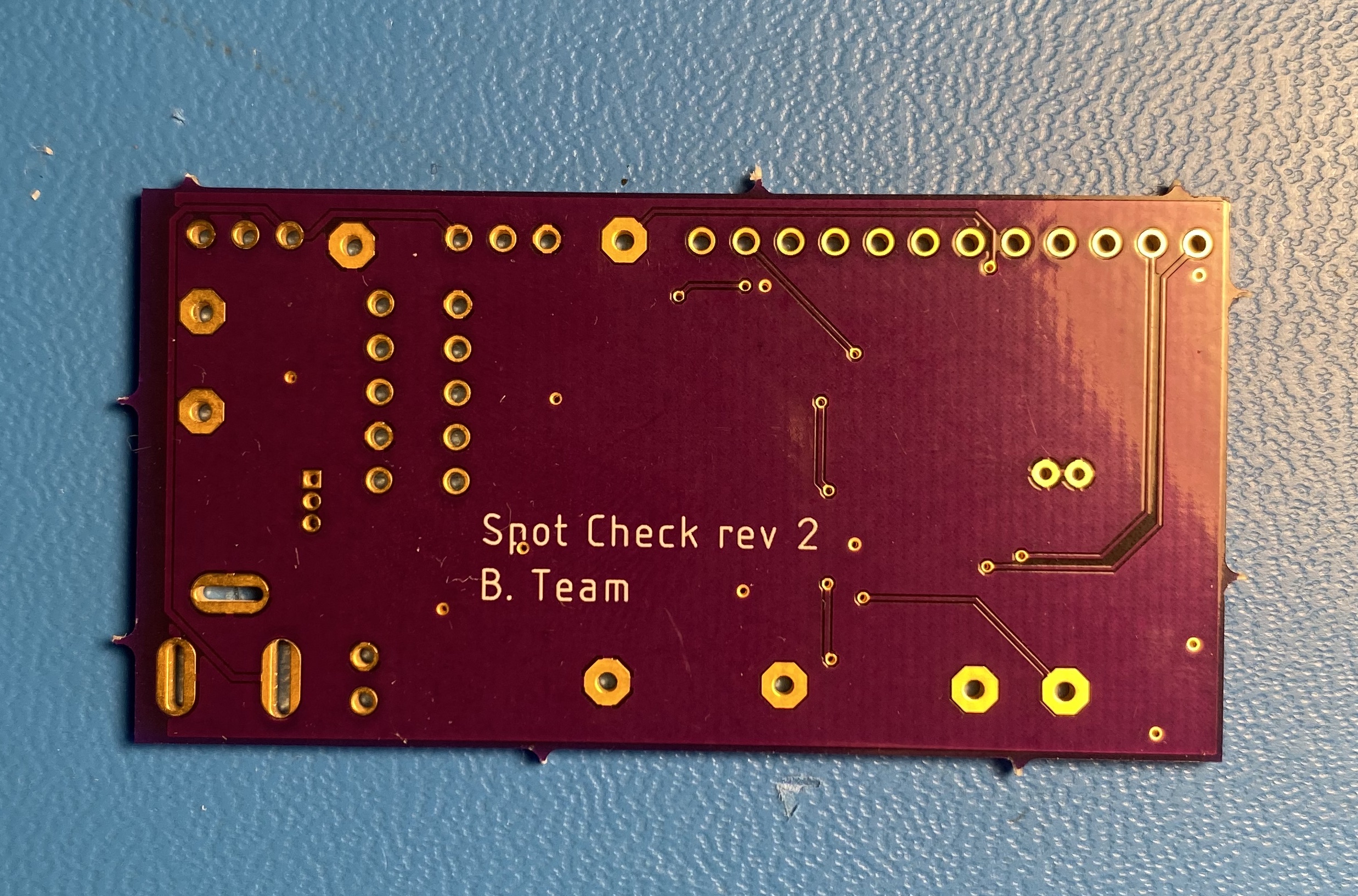
Since the layout was so simple and I left plenty of room around all of the components, routing was a breeze. I only needed a two-layer board, with almost the entirety of the bottom layer dedicated to a ground plane. The few traces I did lay on the bottom I made an effort to concentrate around the board edges or in small lengths to keep the largest continuous current return path in a big center ground pour where most components were.
I used 14 mil power traces for the 5V from the barrel jack, 12 mil traces for 3.3V, and 8 mil traces for signal lines. The 14 mil for 5V was to support any high current that might be pulled by the LED strips, but the 12 mil for 3.3V was overkill but easy to fit so I didn’t mind. 8 mil was a bump up from the board house minimum of 6 mil since again, I had the space, and no reason to push up on the limits if not necessary.
Assembly
First assembled board (sans ESP-32 while I was waiting on it from backorder)
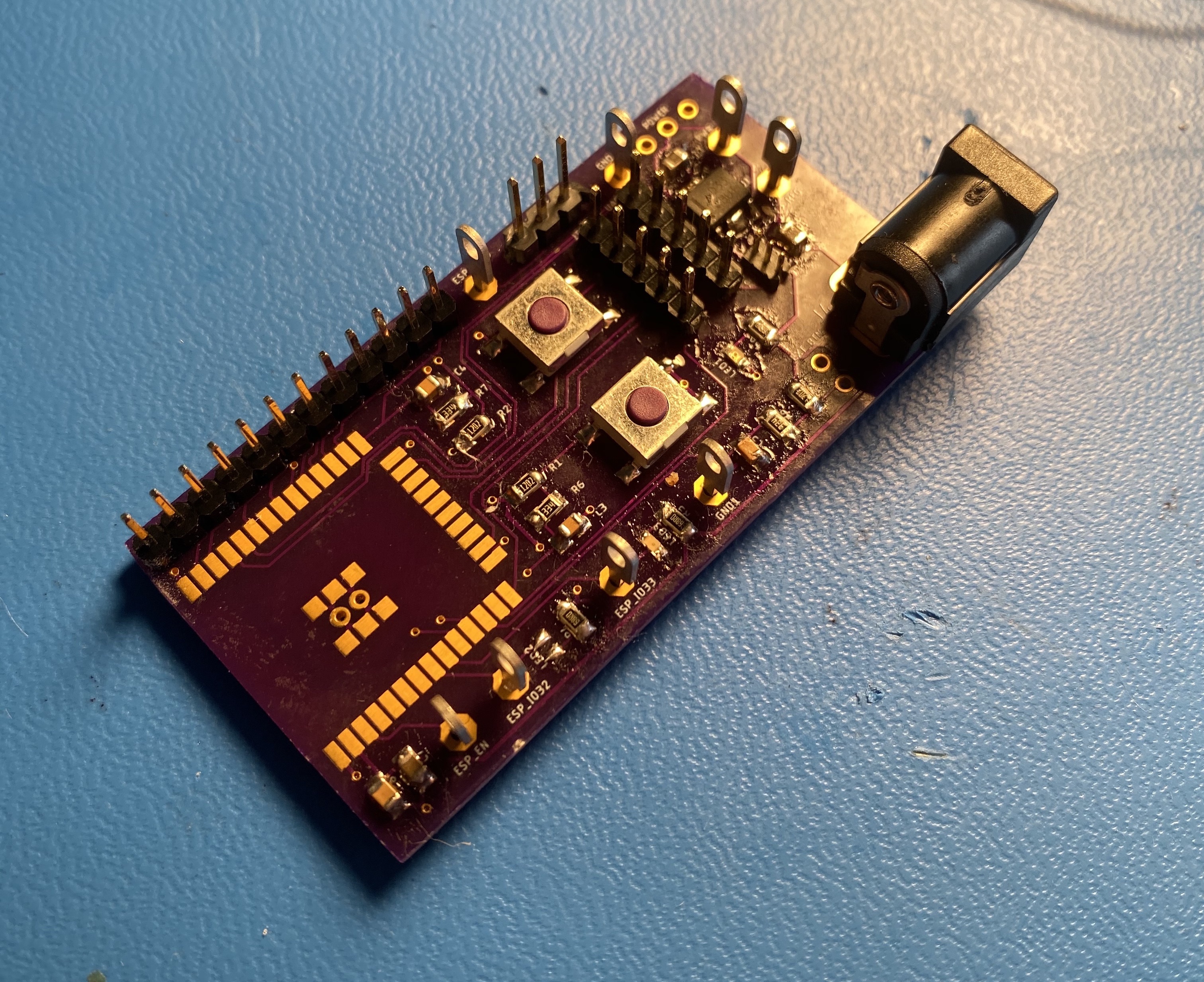
This was my first hand assembly of SMT parts. I deliberately chose middle-of-the-road 0805 for almost all passive footprint sizes. I went with 0603 for the LEDs to see if could drop down another size in the future, and they went well too. The voltage regulator IC was an HSOP which was basically the same sizing as 0805s for the corner pads with fat ground tabs in the middle of both sides. I was interested in how well the ESP-32 would hand solder with its castellated edges, but drag soldering with a good amount of flux and a knife tip on the iron worked wonderfully.
One of the things I wasn’t great at was part alignment while soldering the first pad of a 2-pad part. Even with the flux holding the part mostly in place and aligned on the pads, the first solder joint would always suck the part towards the iron with the surface tension of the melted solder. I’m sure something in my technique or approach wasn’t correct, but I think some more practice will also help.
In parallel with this project, I’m developing a small PCB that will need a very fine-pitch connector soldered with connectors inaccessible from the top or sides (which I’ve now finished with a writeup here). That means hand-soldering is a no-go. To prepare for assembly on this board, I wanted to practice reflowing with one of the Spot Check boards.
The second Spot Check board with SMT parts soldered by reflow rather than hand (buttons omitted because of wrong orientation outlined in Mistakes section)
I ordered a simple electric skillet off of Amazon (this one, but most any will do) and some kapton tape from McMaster-Carr. I laser-cut a stencil in the Kapton tape following this guide, and it turned out fairly well. My solder paste application with the stencil could have been a bit better but turned out pretty well-aligned from my first try.
The solder paste I ordered was non-leaded, but the element mixture supposedly had an even lower melting point than leaded solder paste, so I was optimistic that the heat plate would get hot enough to reflow. For small projects like Spot Check and the other board I’m working on, I’m not worried about multiple heat-zones - any joint issues I can touch up by hand.
The skillet heated up wicked fast, and I almost burned the board it reflowed so quickly (like 45 sec to 1 min from turning on)! I haven’t assembled the remainder of the through-hole components on the second Spot Check board since I don’t need it right now, but it was a good practice run for stencil cutting and reflowing simple boards at home. The solder joints also look much cleaner than my hand-soldered ones.
Mistakes and rework
The first issue I ran into on board bring up was that all of the power test points were reading 0V even with the power supply plugged into the jack. By working back towards the barrel jack and probing along the way, I realized that the power and ground of the barrel jack itself were shorted. Either my power strip plugged into the wall or the power supply itself was helping limit current because I thankfully didn’t trip any breakers.
I had triple-checked the pinout for the schematic symbol and board footprint for the power input so I was pretty sure I didn’t get pins switched around. My first thought was that I didn’t indicate something correctly in the gerbers, leading the board house to link the drilled and plated power hole on the PCB to the ground place. I then tested for continuity in the power jack drill holes on an unassembled PCB and there was none, so the bare board itself wasn’t an issue.
After getting the barrel jack part desoldered completely, I realized that something had happened in the soldering process that had broken the plated power hole into the ground plane since the jack part pins were still correctly isolated. I’m not sure how this happened, since the solder was a pretty straightforward ordeal and I didn’t tear the holes up until I was desoldering. I fixed the issue by bending out the single power pin of the jack so it wasn’t inserted into the board, then soldering jumper wire from this pin to another power pin on the same net. While ugly as hell, it got the job done (I only picked up 28 gauge enamel wire much more suited to rework after the fact).
The second issue was a much dumber mistake. In schematic capture, I didn’t look close enough at the orientation of the pushbutton schematic symbols compared to the pins in the layout footprint. Instead of tying the two internally connected button pins for each side together with a trace, I tied both sides of the button together. That meant it was permanently shorted to ground whether it was pressed or released. I fixed this by desoldering the button, rotating it 90 degrees, and bodging solder and some wire snippets to the originally intended pads on the board. Again - ugly, but efficient.
Next steps
After getting everything, including external buttons for user input, soldered and inserted into the prototype enclosure, I finally had a full, working Spot Check system. Unfortunately, during the process of drilling holes in the enclosure for the power toggle switch and jack output, I must have rubbed the LED strip board that was inserted just enough to knock a few solder joints loose. After power-up, the bottom row of LEDs is no longer illuminated.
I’d like to say that this was the straw that broke the camel’s back, but if I’m being honest, it happened before this point. The LED strips in their current design are just too unwieldy and fragile to be worth using. If it were a great UX then I’d put more work into shoring up their assembly and insertion, but since I still hadn’t come up with a good way for the user to trigger the forecast fetch and scroll from afar, I don’t think it’s worth it.
I’ve decided to switch from a medium-scale, distance-viewed ticker with LEDs to a close-viewed screen. I’ll be using an e-ink display for the UI aspect, of which there exist a few libraries for driving with an ESP-32. There will certainly be more firmware work for the change in the UI interface, but I decoupled the component logic enough within the current firmware that most of the application code can stay the exact same going forward.
The new board design mentioned in the reflow portion of the Assembly section was in reference to the ESP-32-to-e-ink PCB I’m currently working on. There are multiple different voltage levels that e-ink displays require, along with an irregular set of data pins.
The transition to a smaller resolution screen fixes my UX conundrum of how the user interacts. Now they’ll be able to press a button and read the forecasts on the screen right in front of them, rather than the low-resolution scroll across the LED strip ticker. Two bonuses are that the low-power aspect of e-ink will allow me to run this whole system off of a battery, not wall power, and the size/resolution of the e-ink display will fit much more information than the LED strips ever could.
In the spirit of designing and engineering, it’s only fitting for me to move the goalposts now that I’ve arrived at the end goal that I set at the beginning of the project.