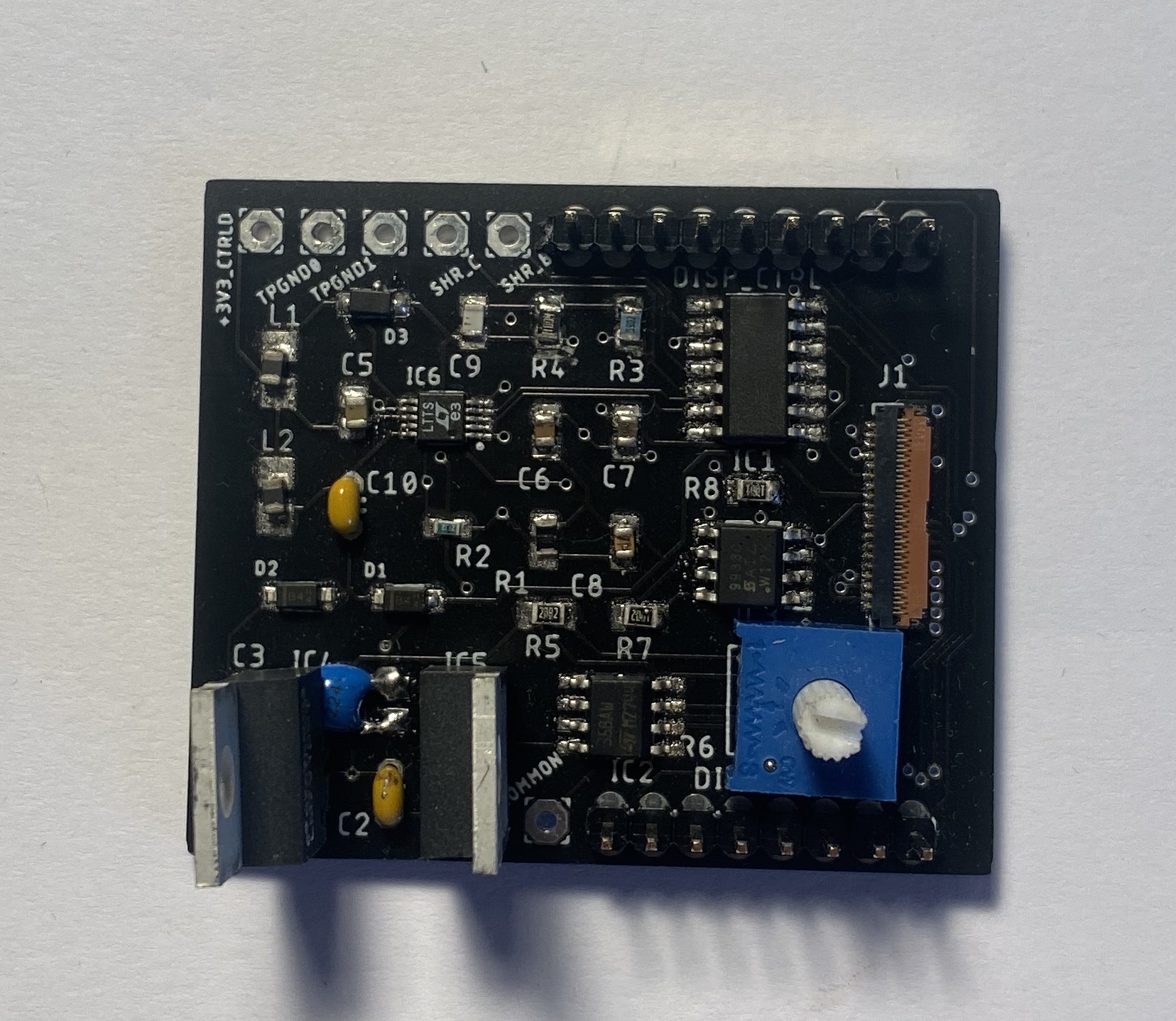
e-ink display driver board
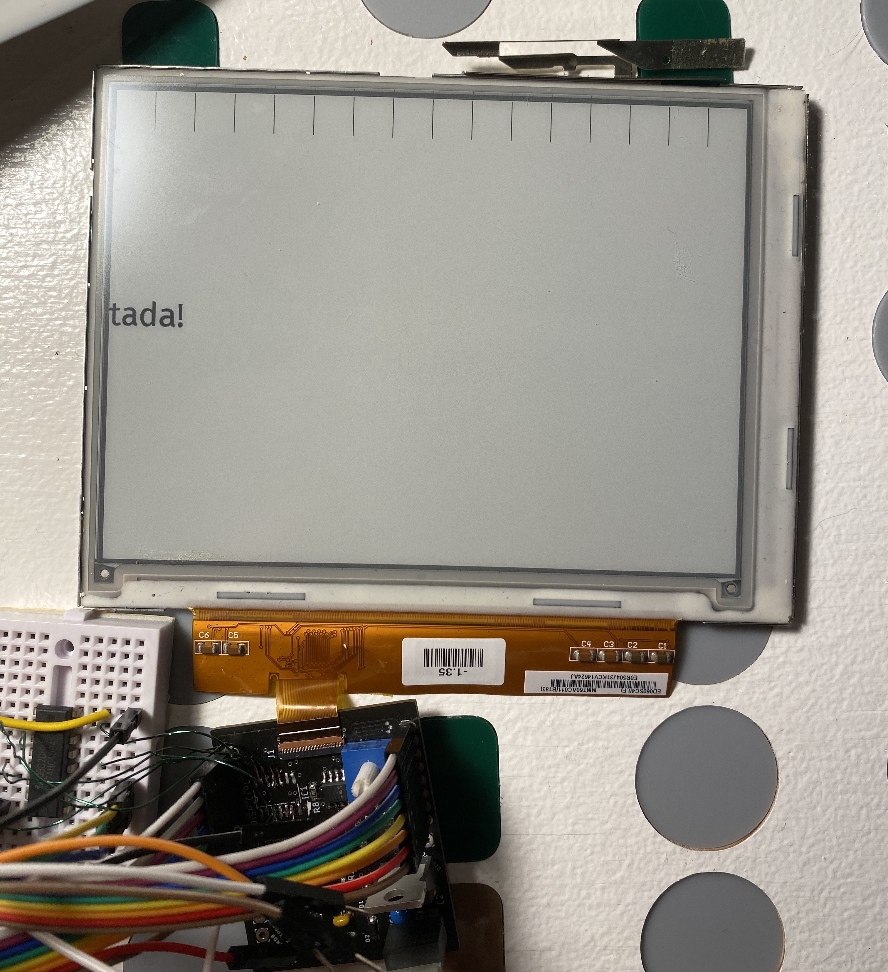
A generic e-ink display driven by my board (albeit with some rework, see Bringup section)
As I outlined at the end of my most recent Spot Check project update, I decided to switch to an e-ink display instead of the LED matrix with scrolling text for displaying surf conditions. I won’t go over the reasoning again, but that meant I needed to update the hardware to support the more complicated circuitry of running an e-ink display.
I didn’t want to buy one of the all-in-one Waveshare display + driver board packages because that would be A) boring and no fun and B) more expensive than building one myself. There are a couple of open-source e-ink firmware and hardware projects in the wild but epdiy was the one that I referenced the most to ensure my design was realistic.
Two other great resources for e-ink support are the EssentialScrap page for the actual waveforms needed and the SpritesMods postings for power and driving circuitry.
I performed schematic capture, component selection, layout, and assembly based on my own knowledge - the above resources were merely used as references as an unofficial “datasheet” for the displays.
I bought a used ED060SC4 from eBay for around 15 bucks which used to be in a Kindle. The ED060SC4 isn’t the biggest nor best resolution, but it’s kind of the “OG” when it comes to e-ink displays and has been better tested and documented than some of the others.
Schematic
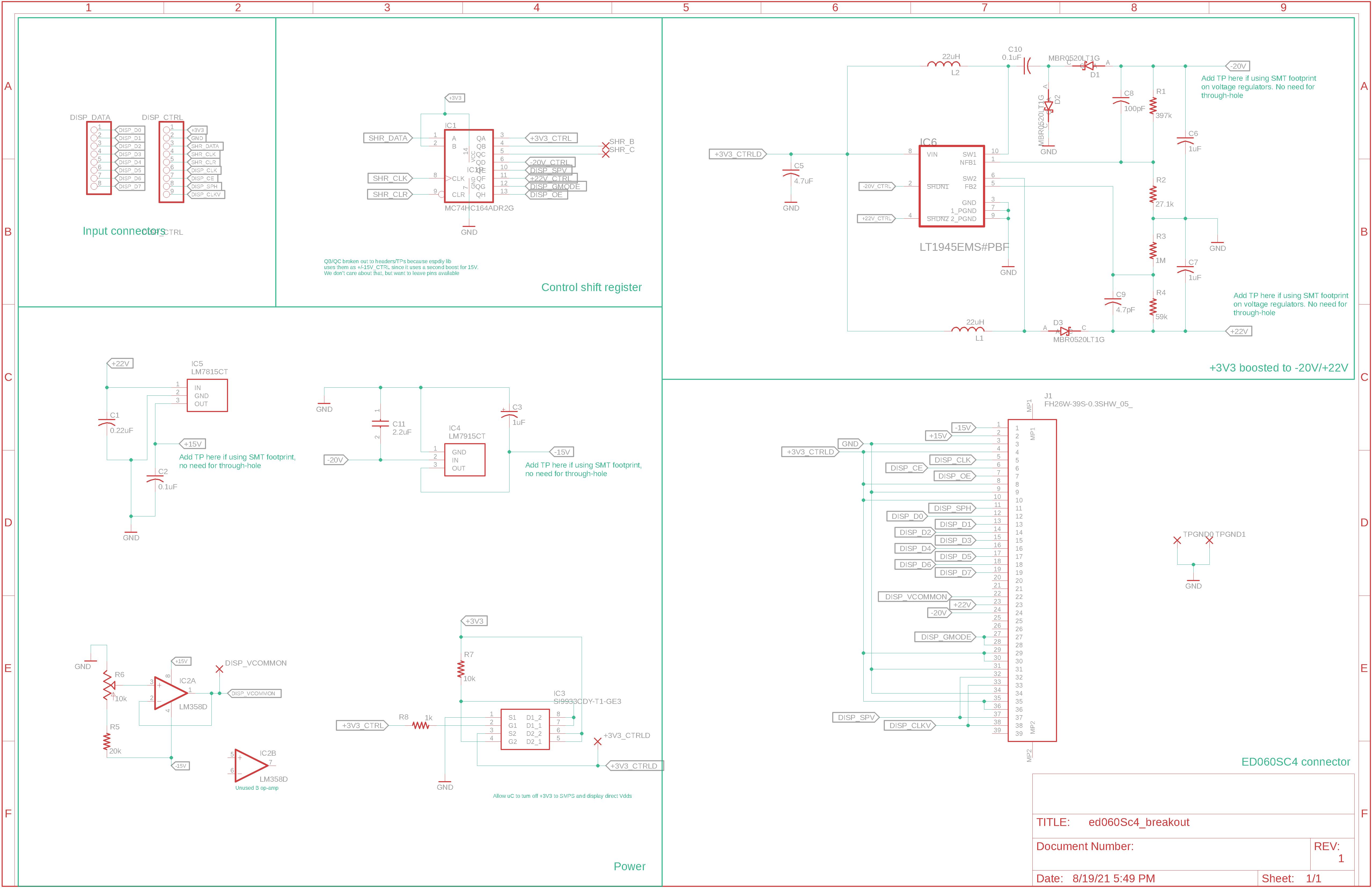
Input connectors
This board was intended to do everything that a microcontroller couldn’t do to drive an e-ink display, but nothing more. That meant I wasn’t trying to design a full board solution but something more akin to a breakout board. If I could have breadboarded the design to test it first I would have, and then integrated the micro in a full board design and called it finished. The ultra-fine 39-pin FPC connector didn’t leave that as an option, unfortunately.
Because I was aiming for maximum flexibility, I broke out access to the board power and signal lines with simple headers in no specific footprint. That meant I could use any microcontroller with the correct type and number of pins with this board instead of locking myself into an ESP-32 or STM32, etc., dev board footprint.
Shift register
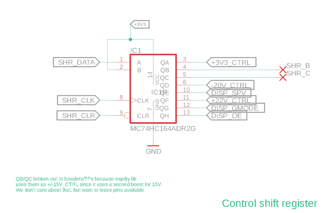
From the get-go I know I didn’t want to pin the signals from the microcontroller to the flex connector one-to-one. I didn’t even know if an ESP-32 had that many GPIO available. The first option I landed on was to use a shift register, and in comparison with the epdiy schematic, that seemed the right call. I didn’t want to route the D0-D7 data signals through the shift register because I wanted the maximum speed of the microcontroller for those. Instead, I used a subset of the display’s remaining control pins which wouldn’t be a factor in a speed bottleneck. I matched the pinout from my shift register to the epdiy one to re-use as much of that firmware without alteration as possible.
Boost converter + power
The boost converter
Power regulation
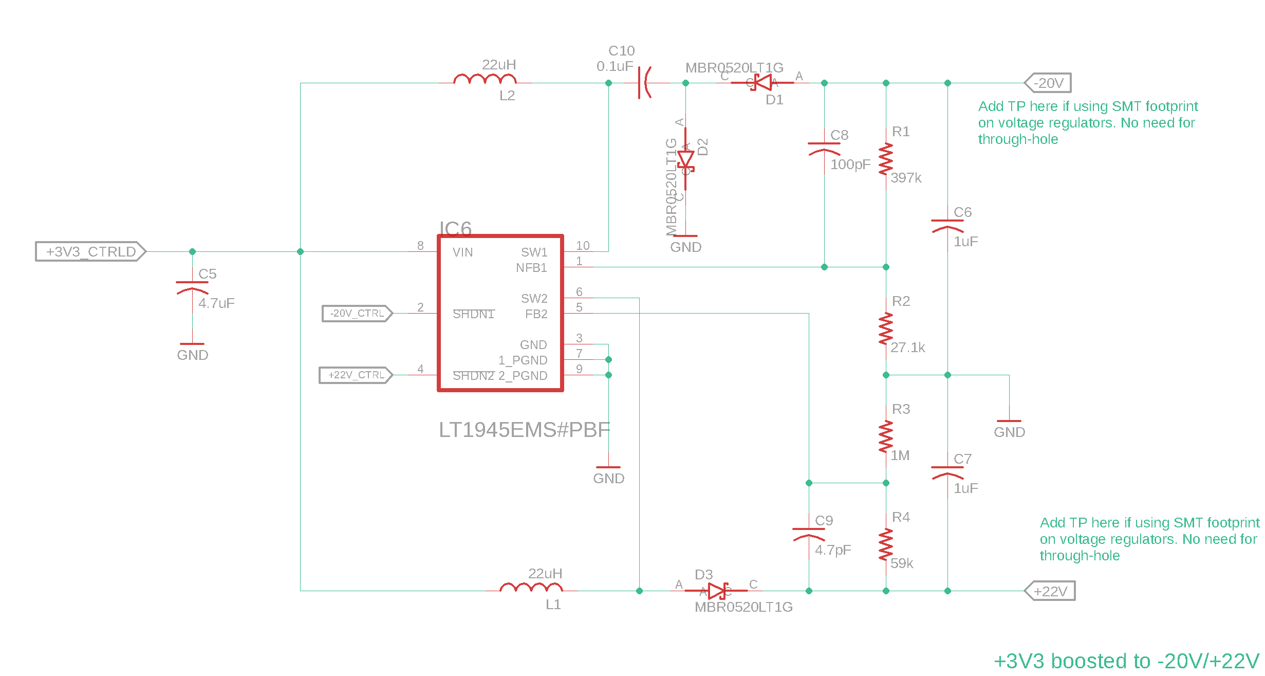
e-ink displays are extremely good low-power devices since they take zero power to retain their display once it’s been set. For the actual transition of a pixel from black to white and vice-versa, however, it uses quite a high voltage. The common consensus is that it takes about +22V and -20V to toggle the gate voltage enough to switch colors.
This meant I’d need to use a boost converter since the only power rail that was available was the 3.3V coming from the microcontroller. This was the first boost converter circuit I had created, but it turned out to be fairly straightforward. Following the equations in the datasheet for sizing the feedback resistor voltage dividers, I was able to come up with resistor ratios to match the correct positive and negative output voltages.
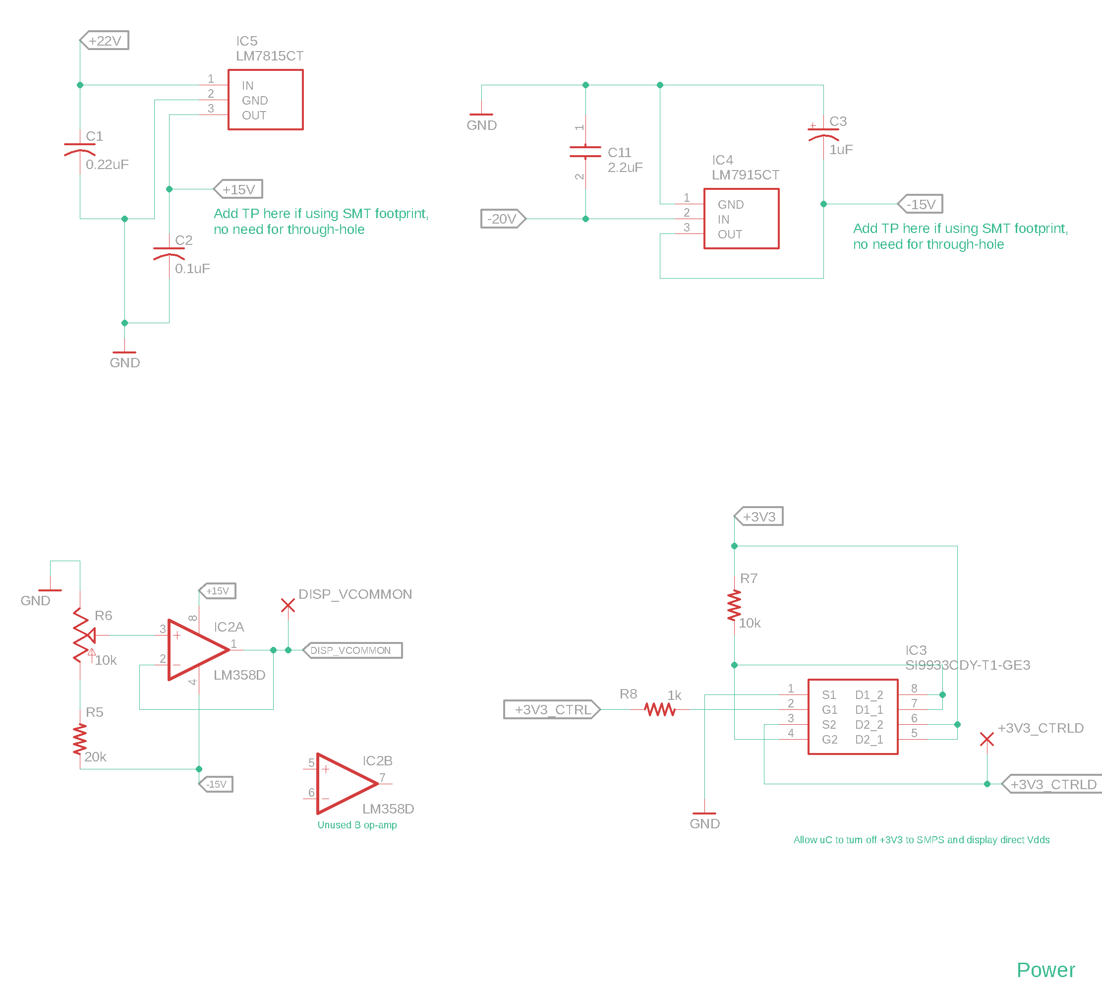
The +22V and -20V rails were both fed through the connector to the display and also into a pair of fixed voltage regulators. These regulators stepped both the +22V and -20V down to +15V and -15V respectively. At first, I was a bit concerned with that large of power dissipation from the large regulators, but the datasheet for the ED060SC4 gave a super tiny max current from the +/-15V, so the actual wattage burned was very reasonable.
I did add one little extra component that wasn’t strictly necessary to the board. Since this design was intended as a driver board for verification of the driving circuitry, I wasn’t concerned with power usage. To plan for the future, however, I added a FET to give the microcontroller the ability to completely cut all 3.3V power going into the boost converter. That’s on top of the boost converter enable pin that was also controller by the shift register. The SpritesMod page was the impetus behind the move, pointing out that the quiescent current of this specific boost converter was not great, and amplified by voltages around the 20V mark meant a decent amount of wasted power even when the enable switch was turned off.
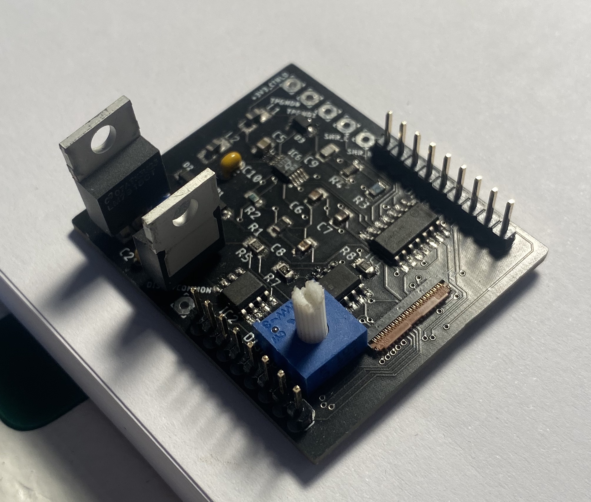
39-pin SMD FPC connector
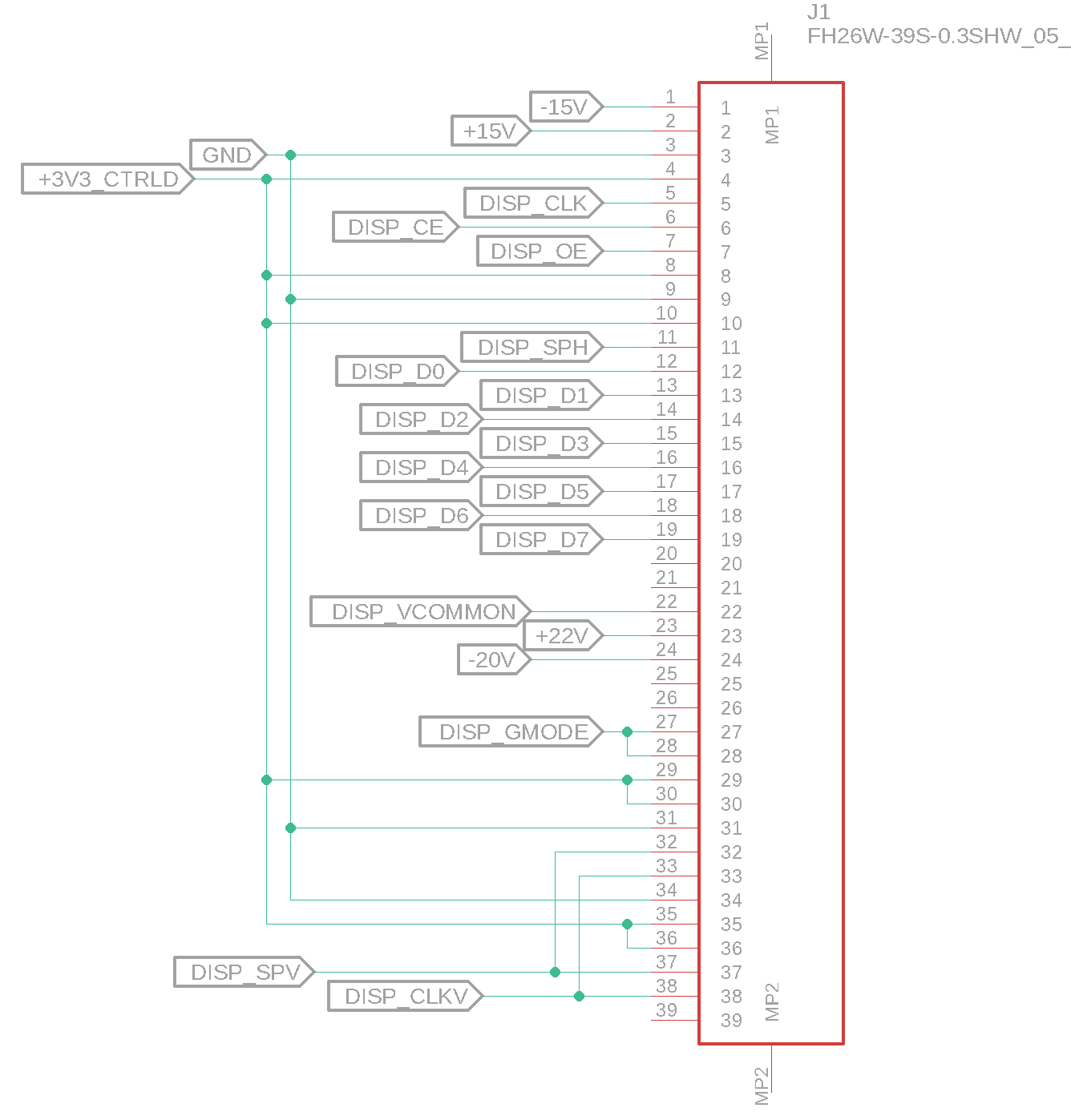
This connector was by far the finest pitch component I’ve dealt with, and the only reason that this test driver board needed to be made instead of using a breadboard for circuit verification first. Thankfully, it was the most-documented piece of information surrounding e-ink displays. It was a relatively simple exercise to look at a pinout diagram of the display cable and map each individual connection to the correct pad.
Board
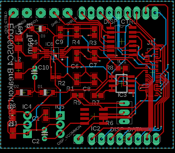
Layout
I went with 0805 sizing for all passives and simple components. I was planning on reflowing most of the board (for the connector mainly) but wanted to keep the opportunity to hand solder if for some reason I could only reflow the connector. I went back and forth on the arrangement of the boost converter supporting components but was pretty happy with the balance I struck between board size and space between pads for routing.
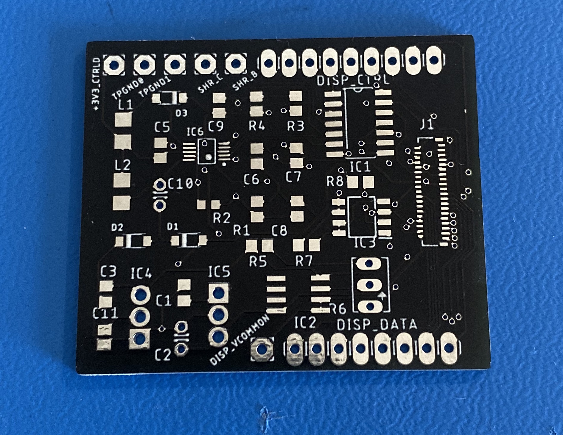
Getting all of the little signals to the correct pads on the FPB connector wasn’t terribly difficult, but there were definitely a few pads near the end that have a bit of wonky routing for the last few mm to get everything in the right spot. I’d say this is probably near the edge of what I’d do with a two-layer board. Anything with either the same pitch and more pads or finer pitched I think I’d need to bump to four layers to get at each pad more cleanly. I was lucky with e-ink displays that not every pin on the connector is used.
I didn’t bother with any mounting holes since, again, this board is just for circuit validation. I tried to keep the headers and test points mostly even and grouped, with the primary goal being that they wouldn’t get in the way with a display flex plugged in.
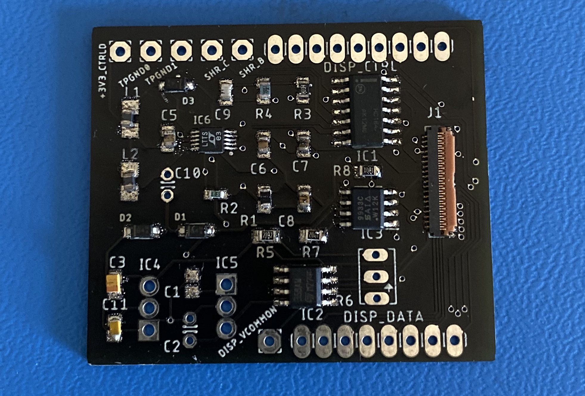
Assembly
I had tested my cheapo hotplate reflowing capability with a previous board and knew it was possible but wasn’t sure how well it would handle something as fine as the FPC connector or 10-pin MSOP boost converter.
I laser cut the stencil out of the thin Kapton tape that I have (see the Assembly section of this Spot Check post) and could see a bit of rough charring around the fine pitch pads but it seemed okay enough. Paste application and reflow went relatively smoothly. I had two loose components when I finished, an inductor and a diode, both on the larger side of the two-terminal pieces. I simply dabbed a bit more paste on their pads manually and reflowed them again.
The board and stencil set up with a surrounding layer of other PCBs for a smooth application
The board post-reflow
In inspecting the joints by eye, I think the Kapton film I’m using is a bit too thin. Either that or I need a better paste application technique. I don’t think there’s enough paste being deposited on each pad to form a really good strong bond, just enough to connect terminals electrically but not very strongly.
I did my best to test the continuity of each pin internal to the FPC connector that would touch the ribbon cable against the actual pad it was supposed to be soldered to. I don’t know how effective of a test this was though since my probe tips could have been bridging two tiny bits or the pressure forming a connection even if the solder joint wasn’t fully realized.
Bringup
I tested the entire board for shorts and ensured continuity on major traces with my multimeter. At first, I just powered the 3V3 pin and made sure all components supposed to be receiving power were.
Since the boost converter enable pins were connected to the shift register, I had to write a quick piece of test firmware to clock the correct signals into the shift register to test the +22V, -20V, and +/-15V rails. At first, I saw the expected -20V and subsequent -15V from the regulator but was only seeing around 3V from the positive output of the boost converter. After re-studying the datasheet, I realized I had flipped my resistors in the ratio voltage divider. Switching the two led to the expected +22V out of the converter and +15V out of the regulator.
Using a modified version of the epdiy firmware, I attempted to get any sort of image or pixel change to appear on my display. What I realized after digging into the purpose of each control signal for the display on the EssentialScrap website is that they operate similar to control signals on something like an SPI bus. That is, maintaining whatever voltage they’re pulled to is just as important as the value of the pin at a certain time. Since I hadn’t looked far enough into the logic of the driving control signals, I had used a serial shift register with no storage. That meant that to force pin three from high to low, for example, I had to clock every other pin value out pin three until I could reach the eight cycles it took to get a new signal on pin three. This obviously won’t work if multiple signals need to change and maintain their value while other pins send data.
There wasn’t a great solution to this. All shift and store registers are sixteen pins since they have one extra pin for the storage function and one extra for daisy-chaining. The footprint on my PCB is for a TSSOP-14 though, and I can’t hang a set of two pins off the top or bottom because I need at least one corner pin on either end of the chip. My current solution is to use a DIP shift and store register and jump the signals onto the PCB with a small bodge wire soldered to the pads. It’s ugly as hell, but actually works.
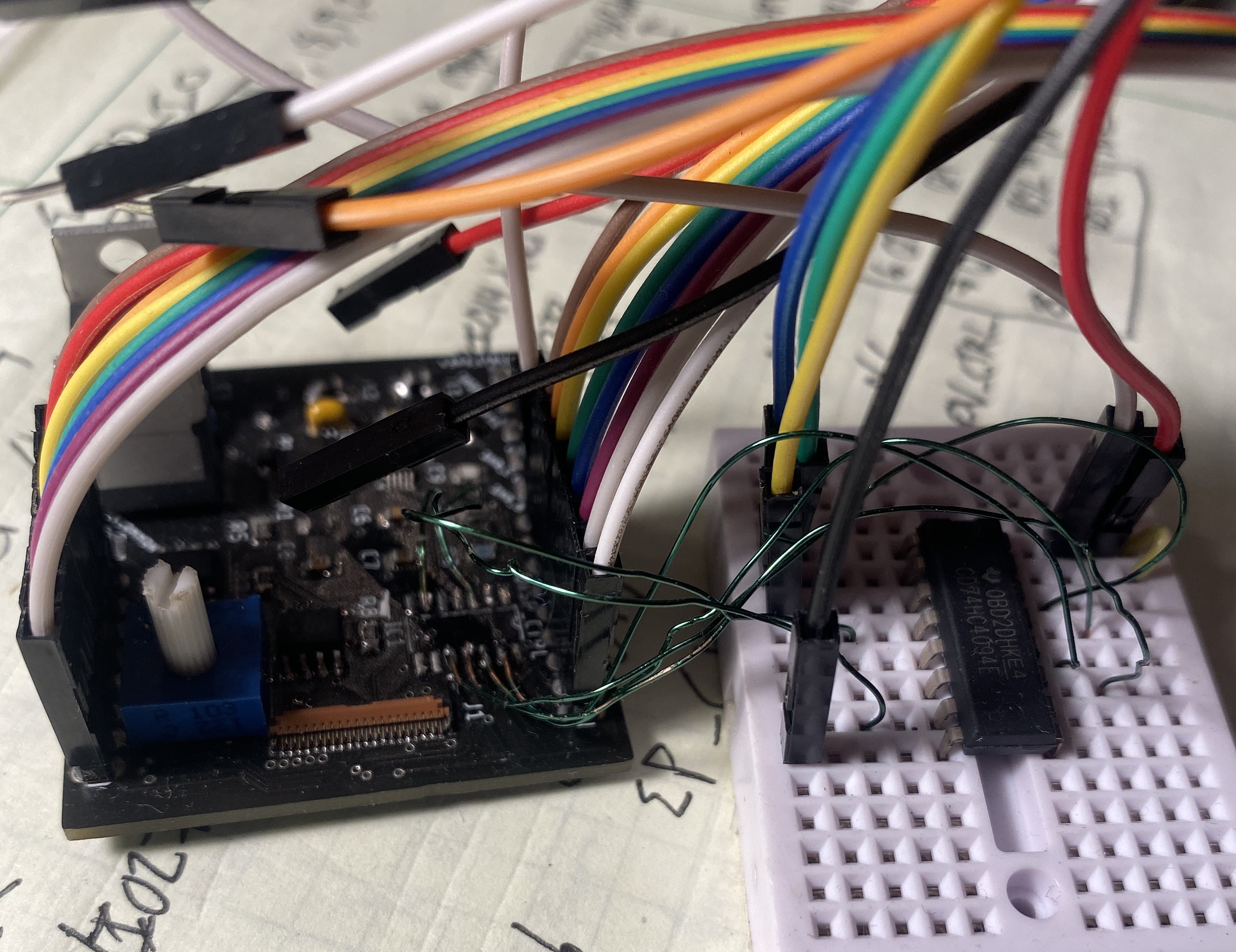
View of the grossest-yet-functional hack job I've ever created
I did a small amount of tweaking within the epdiy source code as well. The firmware designated the ESP-32s IO0 as the pin used to strobe the shift register input data to the parallel output pins. This didn’t work when using a dev board, as the IO0 pin is pulled up externally for use with a physical button for programming. I picked IO014, an easily accessible pin that wasn’t being used, and switched the firmware pin macro.
I progressed to the point where I could see flashing and changes on the e-ink display, but nothing was making sense. Half of the screen was static bars, and I wrote that off as a broken second half of the screen. I saw weird behavior on the ‘working’ half where drawing to any row in a given column of pixels would draw a black pixel to every single row in that column. So attempting to draw short lines spaced out across the top of the display resulted in long, full screen lines. I detailed what I was seeing in this Github issue. After upwards of 8 hours spent debugging this on a Saturday, capturing logic analyzer clips and comparing every line transition to an expected waveform, probing every piece of the circuit I could imagine, altering and stepping through tons of the firmware, I decided to order another screen to sanity check myself.
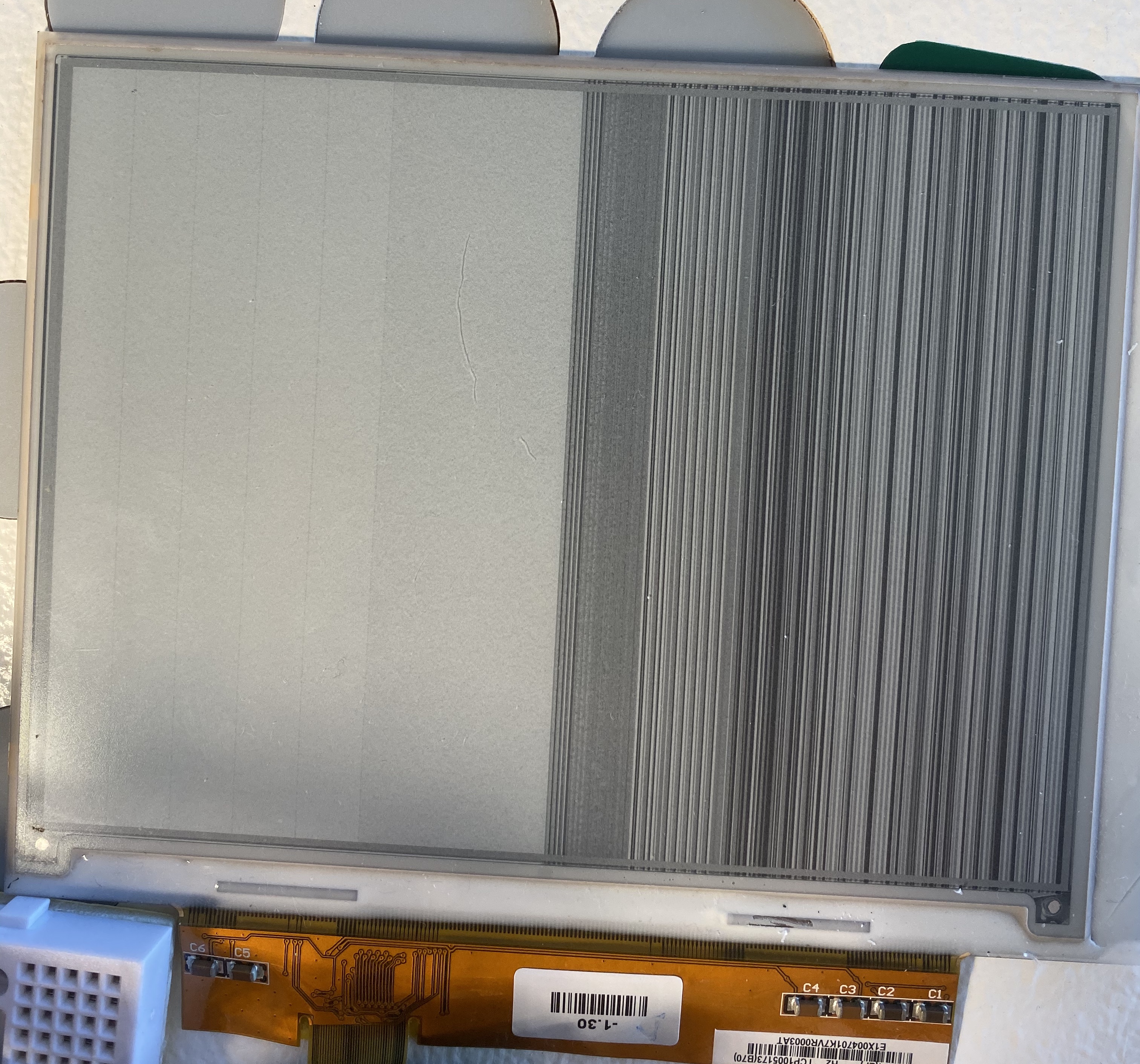
Sure enough, the first screen was faulty. cue enormous facepalm. I was simultaneously very happy and very, very frustrated that I wasted so much time.
The end result was a screen I could update using the epdiy API to draw text, simple shapes, and clear entirely.
Summary
This build did exactly what I wanted it to:
- verify I could reflow the fine-pitch FPC connector well enough to transmit all e-ink driving signals without interference
- verify my circuit produced correct voltages and signals for driving e-ink displays
- verify I could get the epdiy firmware tweaked enough to successfully run and drive dynamic content on generic ~$15 e-ink displays
The next step will be to start a new v3 design of the Spot Check PCB with an intergrated ESP-32 WROVER and components for driving e-ink. I’d also like to include some battery power + charging circuitry, since one of the main goals of the e-ink was to be very low power and able to run without a mains supply.
Since large e-ink displays are still prohibitively expensive, I’ve also come up with some ideas I’d like to try out involving combining multiple of these displays at once.