Light Valve Grid
See a more complete gallery of this artwork on the Second String Studios website
repo containing all firmware, hardware designs, and documentation
Background
‘Light valves’ (also called ‘shutter glass’), are pieces of glass whose polarization can be changed with a voltage differential. It is most commonly seen in large pieces in things like meeting rooms or restrooms where the glass is clear at times, but can also transition to a dark or opaque tint that cannot be seen through.
It’s possible to make panes of this glass of any size, and Adafruit sells two different sizes of small rectangles. The process of making the glass involves sandwiching polarized particles in a thin fluid between two electrically-conductive pieces of glass. When there is no voltage difference between the two pieces, the particles are aligned so the glass is transparent. As charge is applied, they rotate to make the device more and more opaque. Further information can be found in Ben Krasnow’s video on tiny, homemade LCDs.
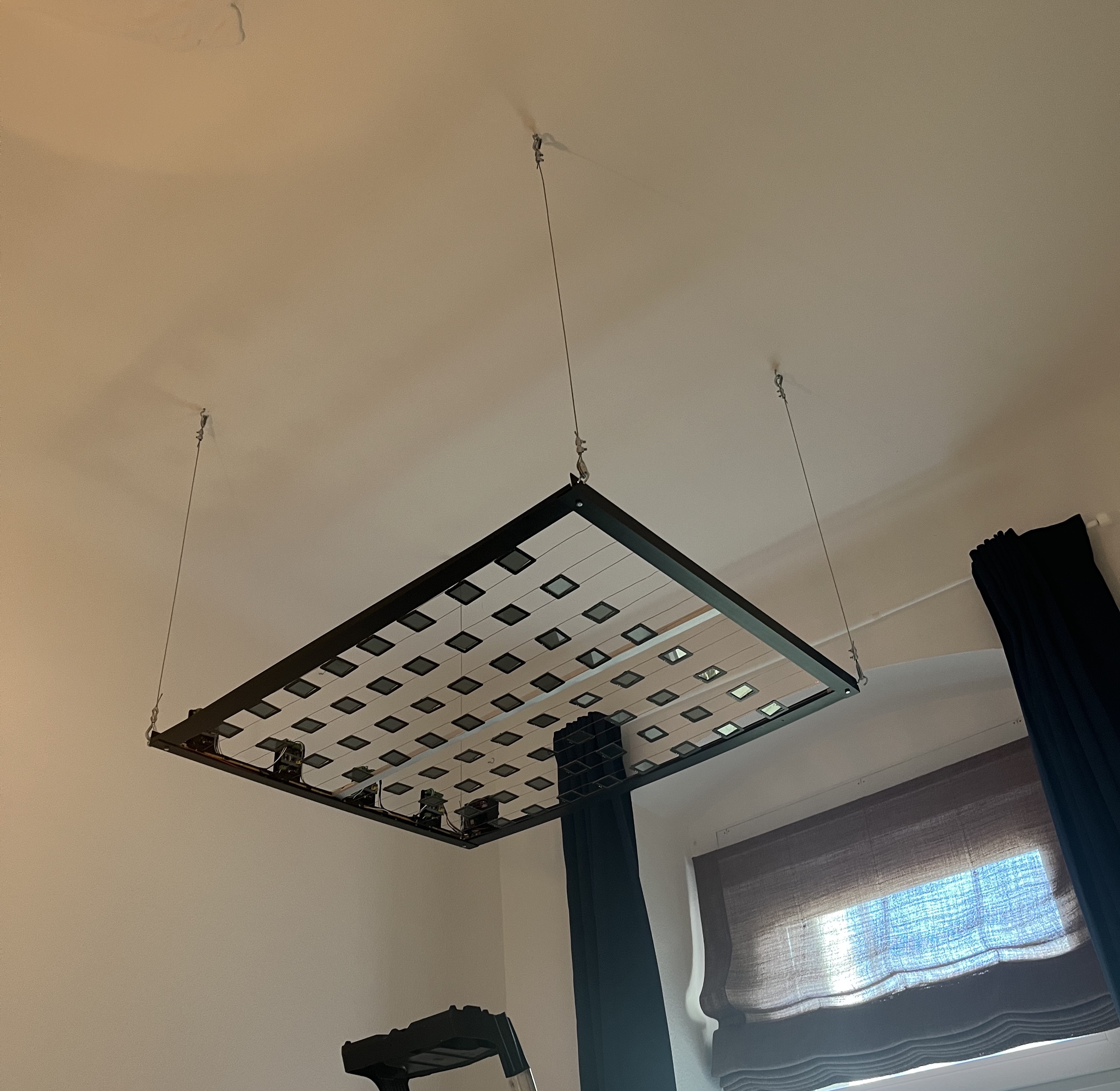
View from below when the grid is set to fully transparent
I first saw the small light valve glass squares about 2 years ago and as I looked into them a little more, I realized that not many people had created anything with them. They seemed interesting enough that I wanted to see what I could make from them.
I found a video of a talk by Mike Harrison about an installation he had created with Jason Bruges Studio using these squares and decided I wanted to integrate them into a project in a similar way.
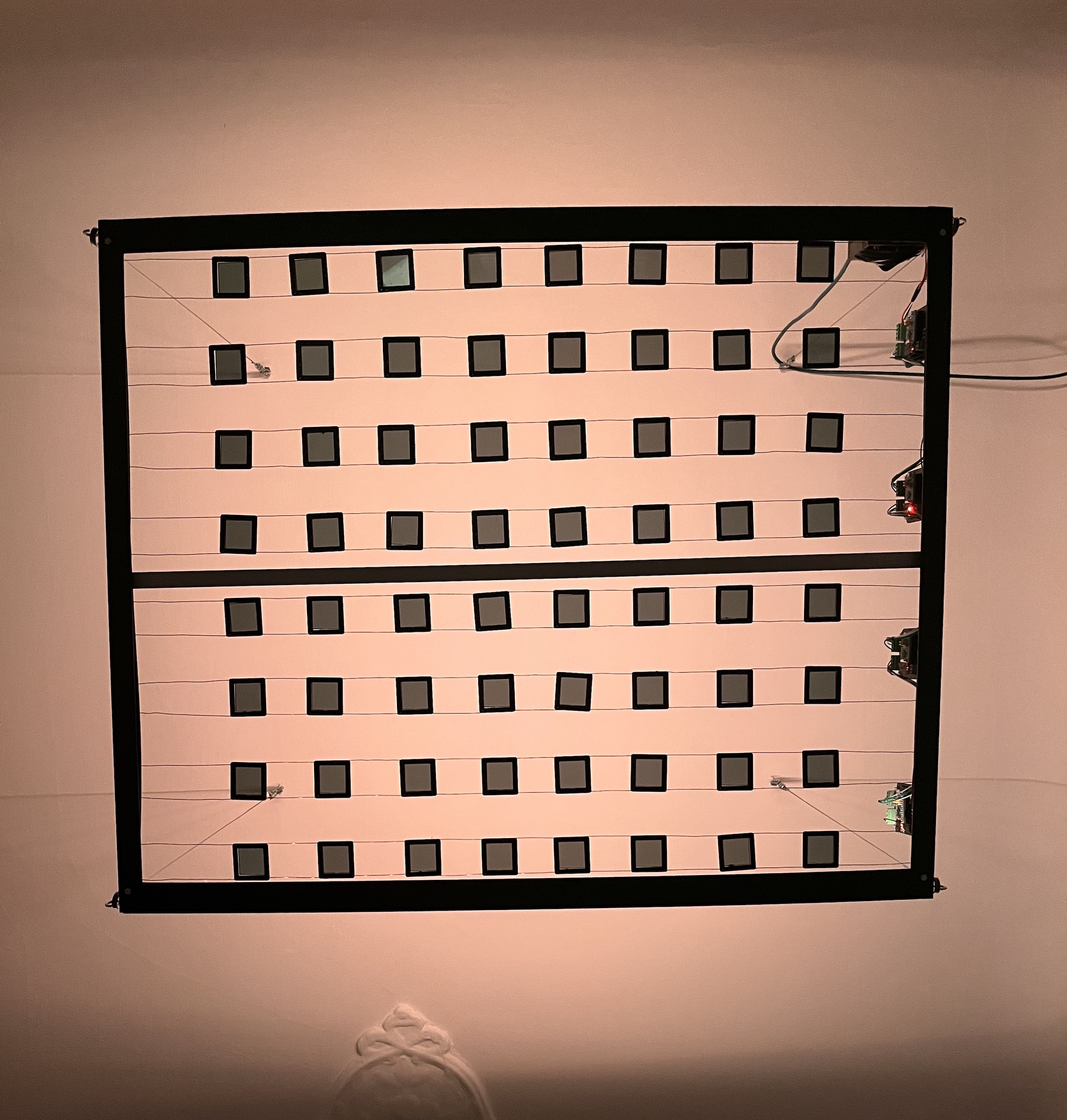
I went through multiple designs for the best way to use these voltage-controlled ‘windows’ so to speak, but ended up arranging them in a very simple way for this first piece. They are laid out in an 8 x 8 grid of glass ’nodes’ that are strung along lines of copper wire hanging in a rectangular frame. The opacity of each node is controlled through TouchDesigner outputting data to the nodes at 30fps.
Hardware
There are four main pieces of the system:
- the content-computer converting the graphical content from TouchDesigner into driver packets on the RS-485 driver bus and transmitting those, along with power, over CAT6 to the hanging grid
- the drivers that convert the driver packets output from the content-computer into node packets on the node buses, 16 nodes per bus (4 total in this piece)
- each light valve node itself consisting of the glass, the controlling PCB frame, and two connections to combined power and data (64 in total in this piece)
- the mechanical grid assembly supporting the node and their wires, the four driver boards mounted, and the two backlight LED strips

Diagram of the overall system and how each hardware sections interconnects
Data and power over CAT6
I created a custom pinout to use all four twisted pairs of CAT6 cable to carry power and data up to the grid from the computer generating the data. I wanted to only run a single cable to the piece instead of having power and data separated and more cluttered.
Below is a diagram showing how all of the necessary signal and power lines were wired into the CAT6 cable and broken back out at the grid. Data flows from the computer at the base of the diagram into a breadboard to combine all of the signals into a single RJ-45 connector, through the CAT6 up the wall and across the ceiling, and is redistributed out of another RJ-45 breakout on the grid.

There are two data signals on the cable: the data stream to the drivers and the pixel data for controlling the LED strips that are laid into the top of the grid. The custom protocol going to the drivers comes out of the computer, but the pixel data is from a standalone Arduino. I currently don’t vary the lighting at all, keeping it at a constant warm white, but could also be integrated to combine lighting and node control in synchronized effects and patterns.
Both data signals are fed through RS-485 transceivers to create a differential signal for the longer cable run up to the grid. Each of these pairs is on its own twisted pair in the CAT6 cable. The other two twisted pairs in the cable carry two 12V and two ground lines.
The 5V needed by the transceivers and Arduino on the transmitting side and the transceivers and LED strips on the receiving side is regulated from the 12V power line.
Driver
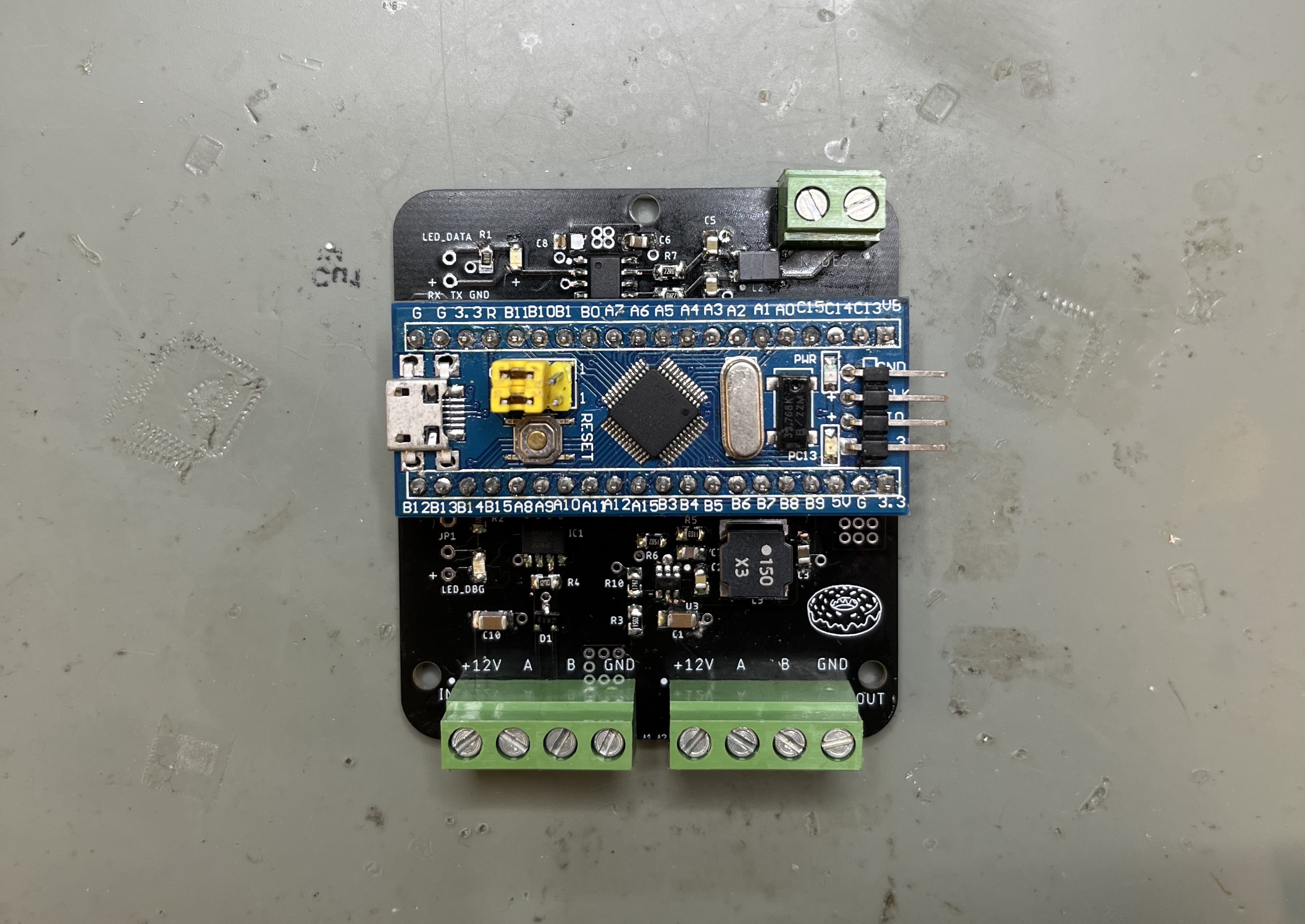
Assembled light valve driver PCB rev 1.1 with STM32 dev board
The driver hardware is fairly straightforward. I opted to use an STM32F103 dev board instead of layout out the chip directly on the PCB. It made development a bit more annoying, but it kept me from having to deal with stenciling and reflowing a smaller pitch IC. I’ve done smaller pitches than the typical STM32 QFP-32, I just didn’t want to deal with it at the time with all of the other moving parts of the project.
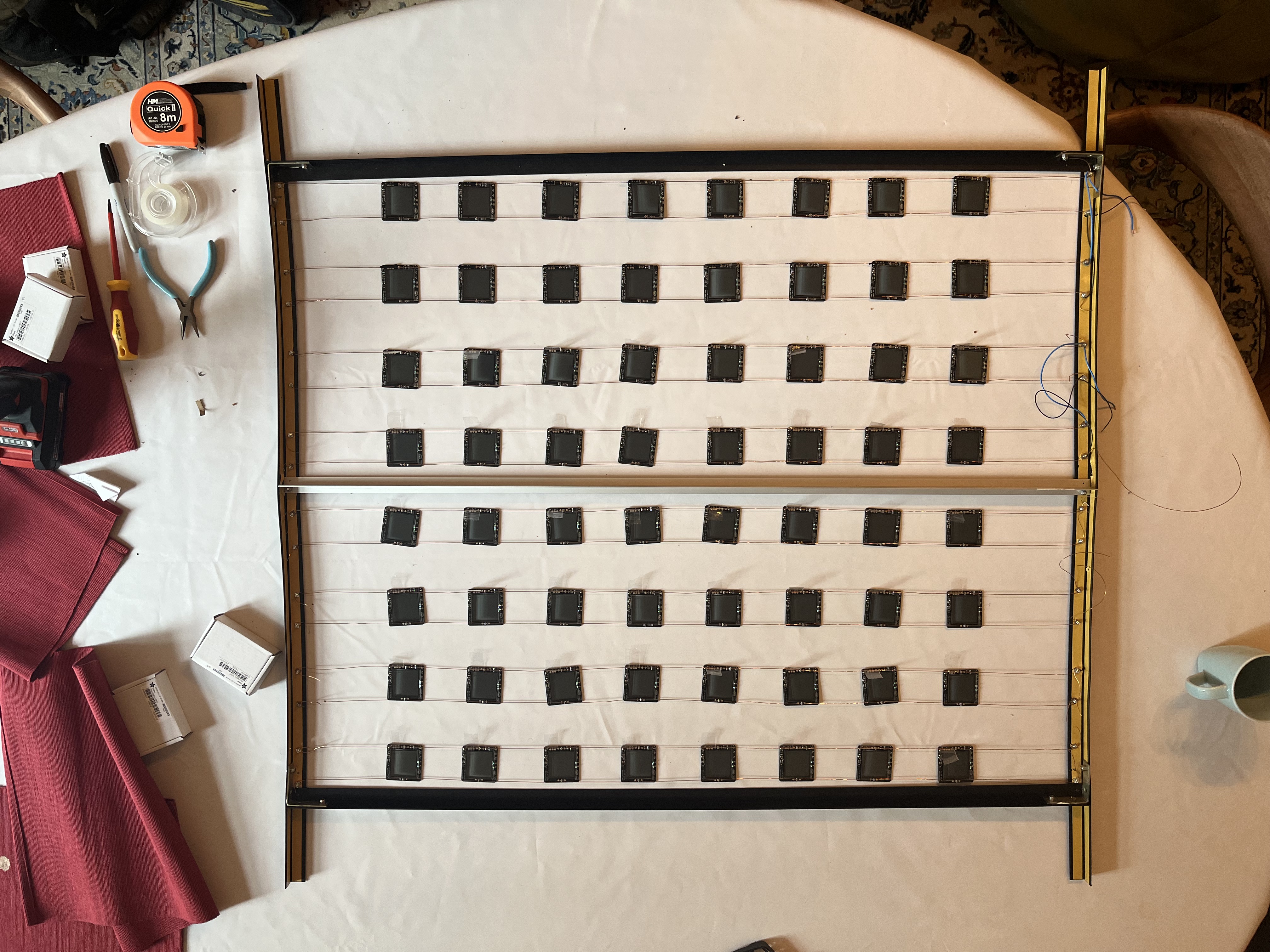
Assembled grid flat on the table before attaching drivers
The purpose of the driver board was to receive packets from the main content computer over an RS-485 bus and translate that data into the simple packet format to send to the 16 attached nodes. The RS-485 input signals, 12V power, and GND were all input into a screw terminal and daisy-chained out a second one.
Board power came from a switching regulator that stepped the 12V power down to 5V to power both the transceiver and the STM32 dev board
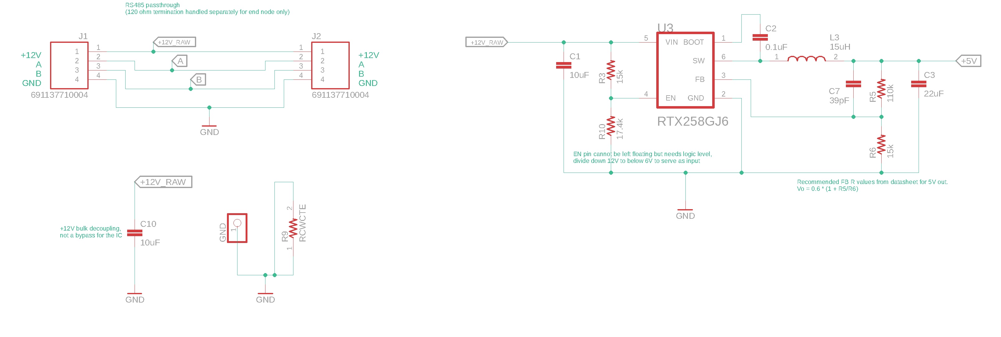
The daisy-chained input/output connectors, the switching regulator, and debug test points
The logic-level output from the STM32 dev board containing the node packet data was boosted back to 12V with a driver IC that was powered from the main 12V coming in from the screw terminal. The driver was chosen with a configuration that included both an inverting and a non-inverting output. These two complementary outputs were the two differential signals fed to the bus that each set of 16 nodes was connected to.
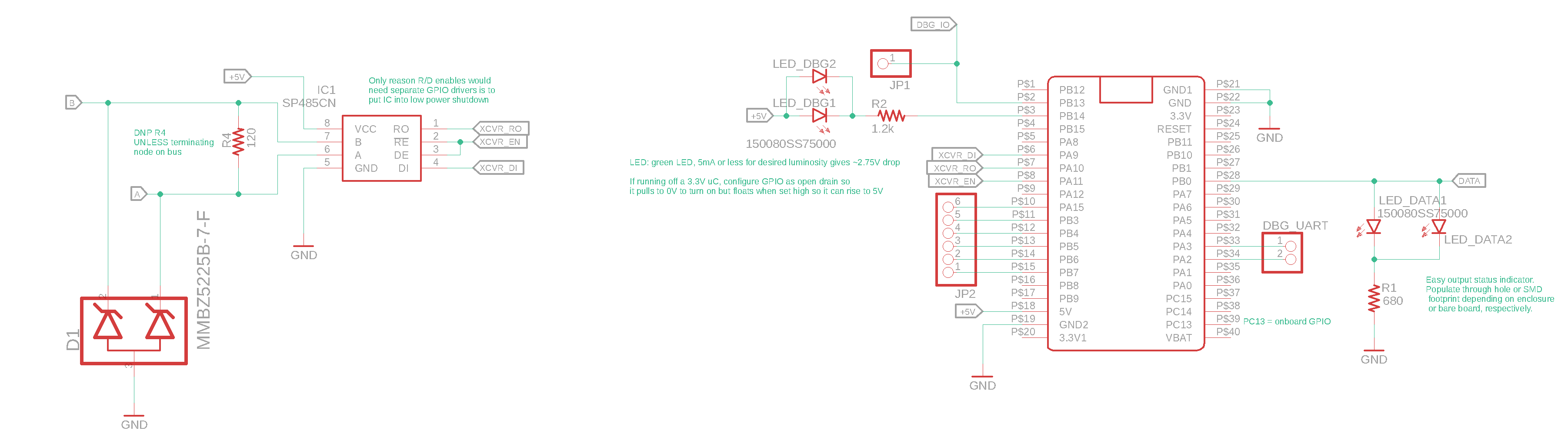
The RS-485 transciever and STM32 dev board
The two output lines of the driver IC pass through two 22 Ohm current limiting resistors and a common mode choke. I don’t know how necessary the choke is, as the total transmission distance of the two lines in this configuration is only a meter or so. It doesn’t hurt to have though.
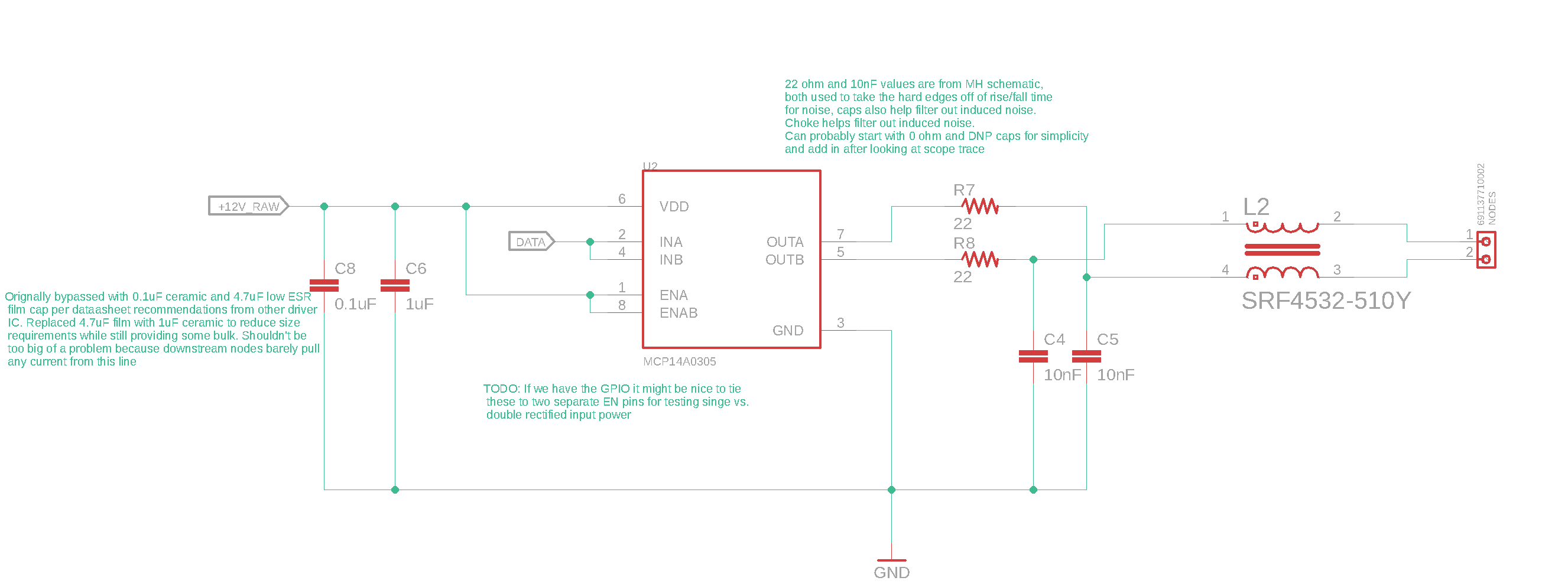
The output line driver, current limiting resistors, decoupling caps, and choke
Node
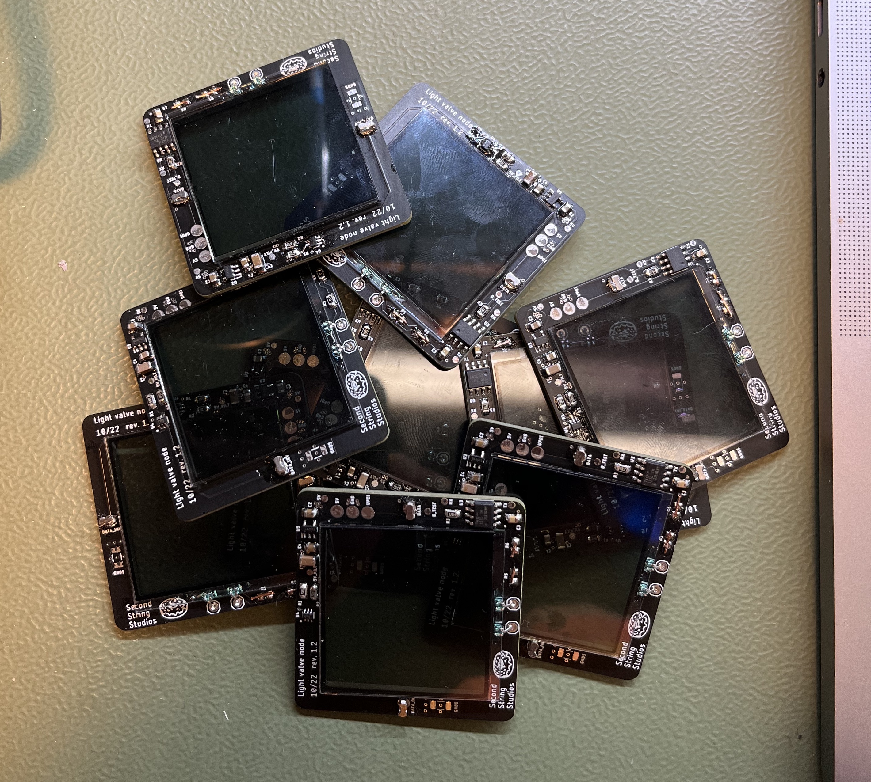
The nodes themselves are very simple pieces. Ideally, they are made as ‘dumb’ as possible to minimize part count and cost, but in practice, that’s harder to do with how they need to be driven. Because the nodes live on buses of 16 nodes each, they need a little bit of processing power to correctly separate and process only the data meant for them. This meant that a microcontroller was needed to decode the simple protocol, rather than sending the raw PWM signal on the bus.
I was optimizing primarily for cost since I was going to be building a decent number of these. The second most important feature of the microcontroller was two individually-controlled PWM channels, which are explained further in the ‘Node firmware’ section below. I looked at some 8-bit PICs and the MSP430 series, but in the end, the cheapest MCU that I found was the ATTiny series. These came out to about €0.55 ($0.60) each in quantities of ~50, came in a SOIC-8 package, and filled the basic peripheral needs.
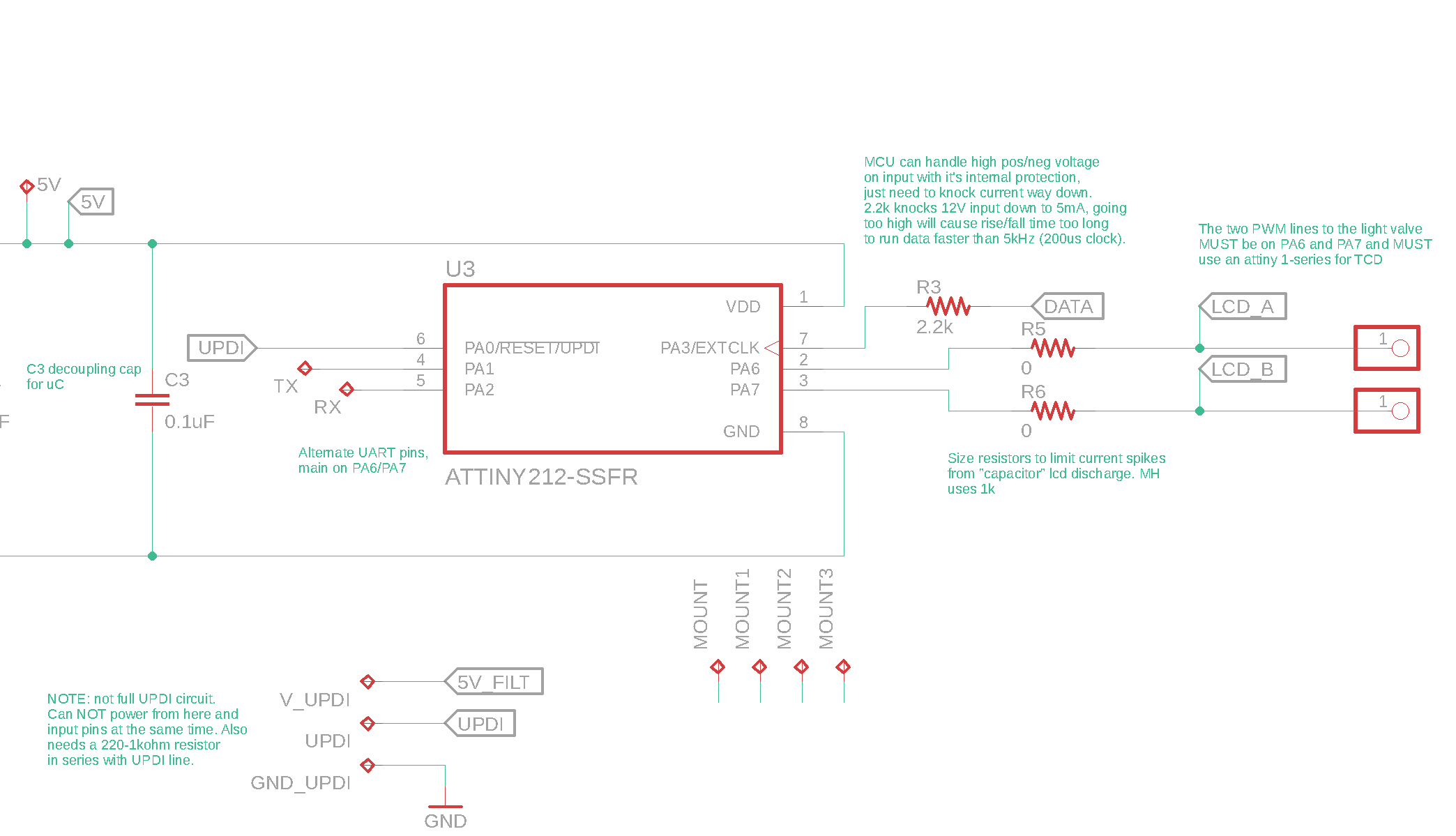
Schematic of the microcontroller and output signals of the node
I also wanted to minimize the number of connections necessary to control each valve. I got the idea for modulating the power line to encode the data on it as well from the previously-linked presentation from Mike Harrison. The two input signals to each node were simply an inverse of each other, so one of the lines was always at 12V. A simple rectifier with capacitor storage could then smooth this dual-phase signal into a constant ~9V signal which was then regulated to a constant 5V from an onboard linear regulator. I put a 22 Ohm resistor on each rectified net to prevent current spikes when charging the rectifier capacitor on first power.
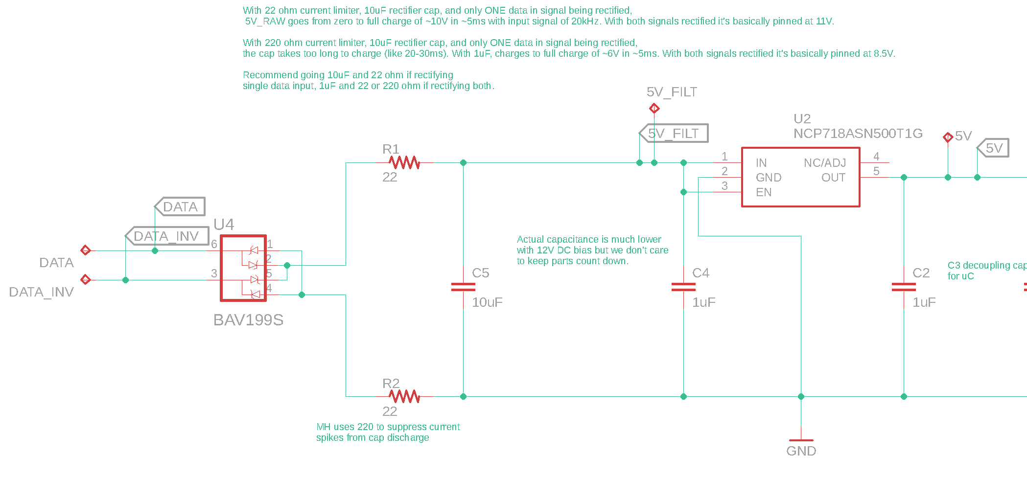
Schematic of the rectified and regulated power and data lines
These two power/data signals came onto the board through two test point pads mounted evenly in the middle of two sides of the frame. These square SMD test points were soldered on as hooks for whatever method of attachment I chose. My initial idea with this project was to hang each node vertically using ~0.5m long runs of super fine steel wire, but when prototyping I realized that the physical component distribution on the node PCBs caused the nodes to be unbalanced, so they all hung crooked. I decided to pivot to the strings of horizontal copper wire going through each test point instead.
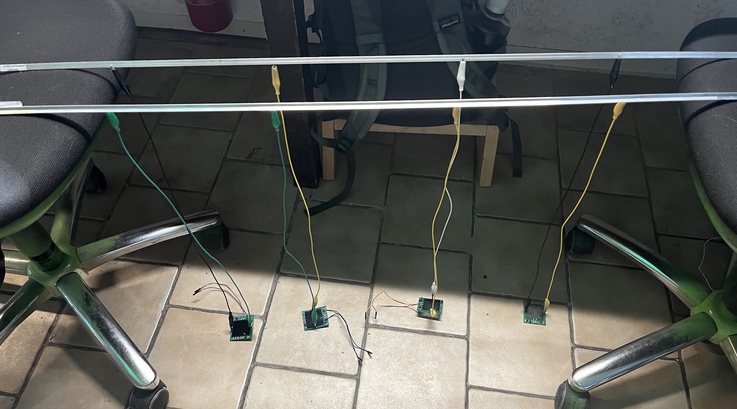
Prototyping the electrical connections and transmission signals when hanging the nodes (rev 1.2). I eventually switch tactics due to uneven node weight.
One of the 12V input lines (it didn’t matter which one, as the data was encoded in the transitions, not the logic level) was routed through a current-limiting resistor directly to an input pin of the microcontroller. The ATTiny series can bleed off the higher voltage level with its internal voltage protection diodes as long as the current is limited down to within its GPIO sink limits. This isn’t a design I would use for a robust product, but works fine for something small in a project like this to minimize parts count.
The dual PWM outputs were routed from the ATTiny to the through-hole connections to the glass through a pair of 0 Ohm resistors. I added these in case I needed current-limiting from the charge-discharge cycle of the glass as the PWM signals oscillated, but in practice haven’t seen any need to increase their resistance.
The newer ATTiny line can be programmed over Microchip’s proprietary one-wire protocol, UPDI. The programming header for this board was simply 3 test point pads (5V, UPDI, GND) that I could lay the pins of the programmer on. I chose this simple implementation primarily to prevent any extra drills to the front side of the frame as an aesthetic choice, but also to minimize parts count.
Grid assembly
The frame of the grid is made out of simple plastic L pieces cut to length. The dimensions of the grid are 1.0 meter by 0.8 meters.
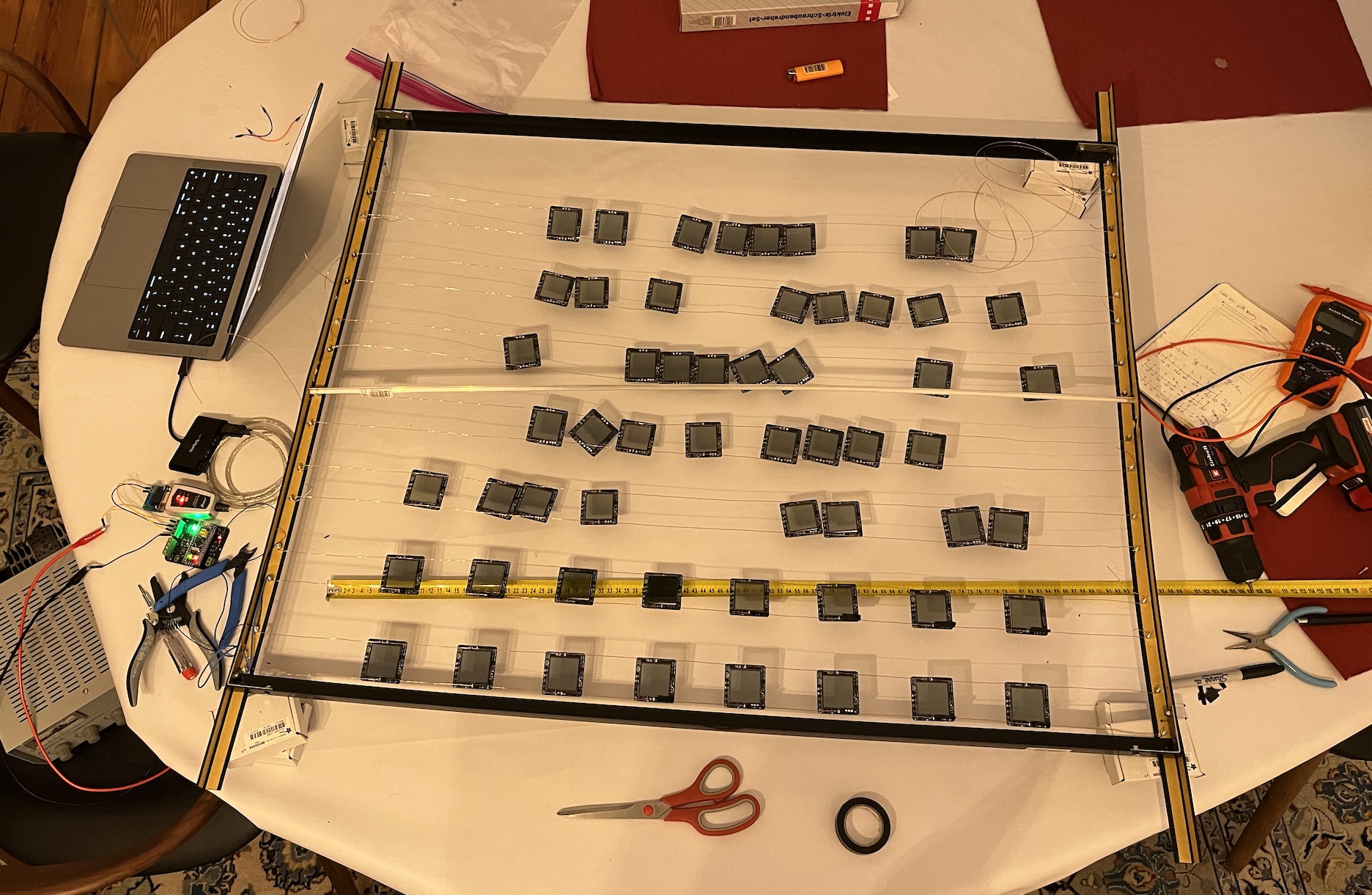
Assembly of the grid rows in progress
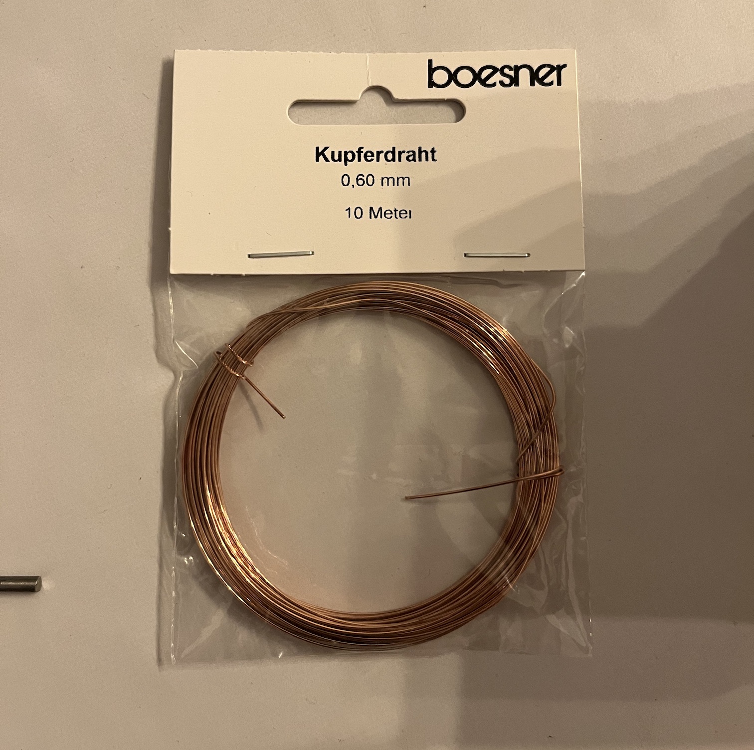
Each row of nodes is strung on a 1m pair of 0.6mm thick copper wire. I wanted to go a bit thinner than this, as at this thickness the wire is hard to get perfectly straight when stretching it and it retains some kinks. The next size down available to me was 0.2mm, however, which was too thin and would snap when I tried to tension it to hang the nodes.
The wire is attached to the grid by wrapping it around an M3 screw on either side of the grid which is screwed through the plastic. A small nut is tightened on top to hold the wire and prevent it from unspooling. The tension of each row is adjusted by turning the M3 screw, but there is a balance between too loose (the wire rows sag when the nodes are hanging) and too tight (the plastic grid frame deforms and bends inwards). The bending can be seen even with an aluminum support rod inserted in the middle as shown in the Driver section above.
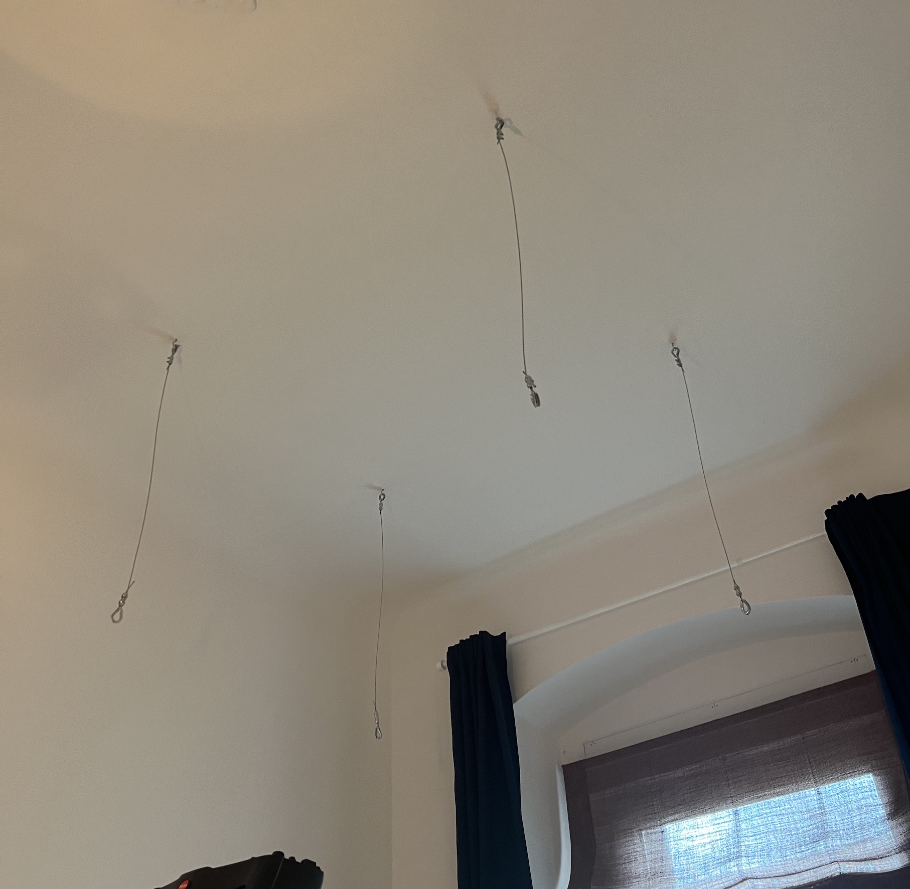
A small threaded hook was screwed into each corner of the frame and hung from four thin metal cables hung from the ceiling. The CAT6 cable run for power and data goes across the ceiling and down one of these cables to the grid.
Firmware
Node firmware
The firmware on each node is extremely simple. It’s a simple state machine for reading in the basic bit-banged protocol coming from the driver. Each node lives on a “bus” of the hanging wires that are attached to the driver. Each driver can address up to 16 nodes in a single packet.
The data is encoded and transmitted with Differential Manchester encoding, which means ones and zeroes are encoded by the length of time between transitions. By using the time between the transitions instead of the high-low voltage level of the signal (which the original Manchester encoding scheme does), the polarity of the two inputs to the nodes is irrelevant.

A diagram of Differential Manchester encoding as shown on Wikipedia
I wrote it in the Arduino IDE for the sake of time and simplicity but manipulated GPIO and other peripherals by register access instead of the Arduino SDK to get the fastest possible baud rate for the driver-to-node communication. I don’t actually think I’m using any Arduino functionality so it theoretically could be pulled out into a Makefile project with the AVR toolchain, there just isn’t much need since even with any included Arduino abstraction the code can fit in flash.
The state machine within the firmware increments based on a simple edge-triggered interrupt. By timing the microseconds since the previous edge, it can tell whether the received bit is a one or a zero.

Breakdown of what each bit in the packets seen by the node corresponds to
The first two signal transitions set the clock rate. That way the receiving code can save the real-time separation of transitions that represent a clock cycle, and then use that value to measure the subsequent transitions.
The first four bits received are the start nibble. This should equal 0xA for every packet and they verify that the clock rate is receiving data correctly.
The next state is the combined node address and data value. This is why only 16 nodes are addressable on a bus, as the higher nibble corresponds to the node address and the lower nibble is the 4-bit value representing the opacity for that node. Once the full byte has been read, the state machine compares its known own address to the received address nibble. If they match, it uses the lower four bits to set the opacity level.
It would be fairly easy to increase this packet size to support more nodes on a single-driver bus, but it comes at a tradeoff of a lower total FPS possible for addressing all nodes on the bus with a single packet (plus I like having it fit nicely into a byte).
There is also a timeout timer that is reset every time a signal transition interrupt triggers. If the timeout expires at any point in the state machine, the firmware will consider this packet corrupt or missing bits and transition back into its idle state.
The logic for converting the opacity level to the actual PWM signals isn’t too complicated but is a bit trickier than expected.
Because the opacity is controlled with a voltage differential between the two panes, one might think that only a single PWM control line is needed while the second pane can be grounded. Unfortunately, a long-running DC bias on the glass is bad for the internal polarization particles, so it must be controlled where the differential can be varied, but has a net bias of 0V over time.
That’s why two separately configured PWM peripherals are needed. See the diagrams below for the difference between the 0V DC bias PWM signals and simply using one PWM signal.

What the combined PWM signals look like when it is one signal inverted and then combined. When the duty cycle is 50%, this correctly results in a net 0V DC bias

The same single channel inverted signal, but at a 25% duty cycle. You can see that there is a bias to the -5V side of the swing because that section of the signal combination is larger.

Two individual PWM channels at 25%. Because only one channel is on at a time, followed by both signals at zero volts, the net combination of them has an average DC bias of 0V while still driving the node to +/-5V.
Driver firmware
The driver firmware is standard STM32 firmware using the HAL and LL generated from CubeMX. I chose to use FreeRTOS for simplicity but it could easily have been done bare-metal. There are four total FreeRTOS tasks, only two of which are necessary for the driver’s functionality:
- input data task
- output data task
- CLI task
- heartbeat task
The input data task uses DMA with the incoming UART channel from the RS-485 transceiver to read in all incoming bytes. It checks to make sure there is a valid start nibble and that the driver address in the packet matches its own address. If so, it pushes the read-in bytes into a queue and signals the output data task.
The output data task blocks on a notification from the input data task that a packet has been received. Once it has, it reads out the actual node opacity data from the driver packet data, packages that up in a node packet (structure described in the ‘Node firmware’ section), and sends it out the GPIO connected to the 12V line driver IC.
The CLI task is purely for debugging and development and implements a few simple commands and responses over a separate UART. The heartbeat task is a simple LED blink to show externally that the driver is still operating as expected and hasn’t encountered any faults.
Software
This project was my first foray into TouchDesigner as the main design and content generator for the piece. I started with a simple python script for generating basic patterns and outputting the driver packets but transitioned this into TouchDesigner to enable more complex visuals.
I created a grid of cubes within TouchDesigner to act as my basic rendering template and then piped each of the generated patterns across these cubes. I developed a basic UI that allows for switching between certain patterns, adjusting the rate or orientation of those patterns, and manually taking control of the nodes to sync better with live content.
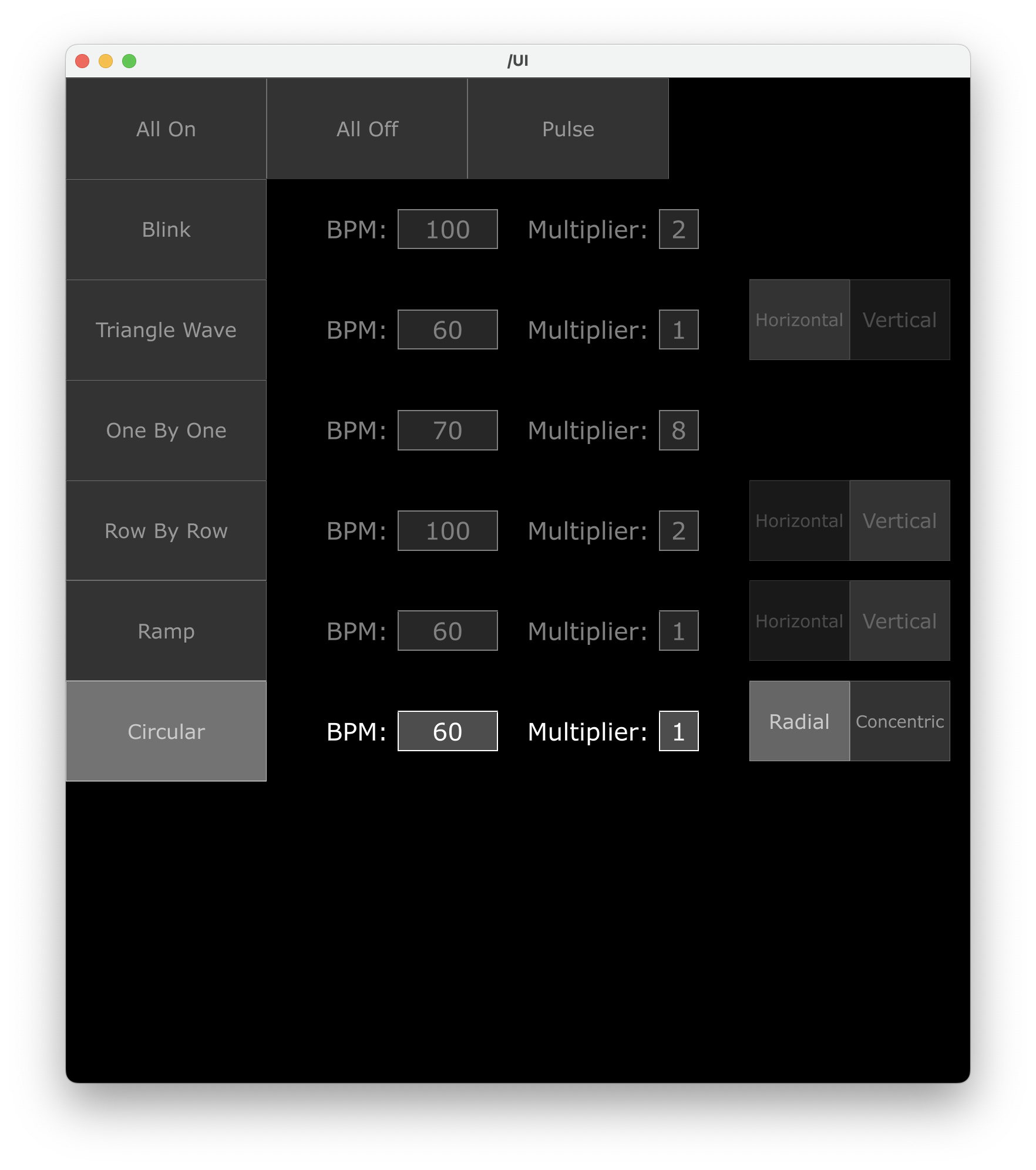
The UI designed in TouchDesigner for changing patterns and parameters
The output of the patterns was broken down by driver channel and inserted into driver packets using components of the python script that I initially used for testing.
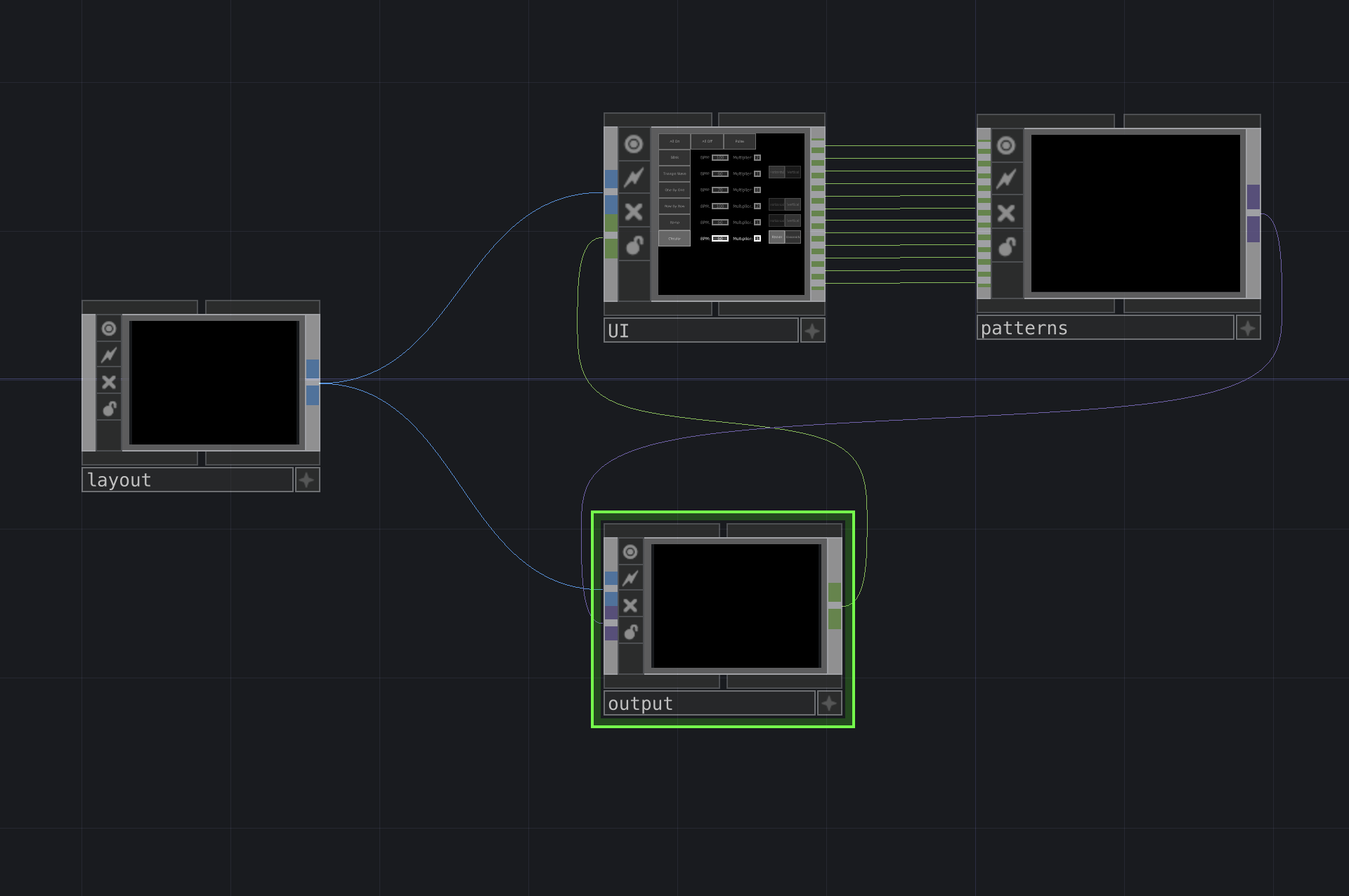
The top level of the TD project showing each functional container